
Key Takeaways for Engineers
- High-Impedance Filtering: 1.00 mH nominal inductance provides superior low-frequency noise suppression for sensitive signal lines.
- Thermal Awareness: The 5.75 Ω DCR provides natural EMI damping but requires careful thermal management at >200mA loads.
- Compact Integration: Shielded wirewound design reduces PCB crosstalk by up to 30% compared to unshielded alternatives.
- AI-Ready Verification: Ideal for low-current sensor rails where impedance at kHz-MHz range is critical for data integrity.
The 784777102 datasheet lists headline numbers designers care about: 1.00 mH nominal inductance, rated current ≤250 mA, and a maximum DC resistance (DCR) around 5.75 Ω measured under the datasheet reference conditions. Those values directly influence I²R losses (reducing efficiency in high-power rails), voltage drop on power rails, thermal rise on the PCB, and the choke’s effectiveness at EMI suppression. This article delivers a practical, test-aware breakdown of the 784777102 datasheet so engineers can evaluate inductor specs and electrical details quickly and confidently.
Sections that follow cover a compact part summary, deep electrical-spec analysis, recommended lab verification steps, a real-world EMI/thermal case study, and a concise selection checklist. The aim is hands-on guidance: understand what the datasheet guarantees, how to reproduce those numbers in the lab, and how to integrate the part into low-power designs.
Background: Part summary & where it fits
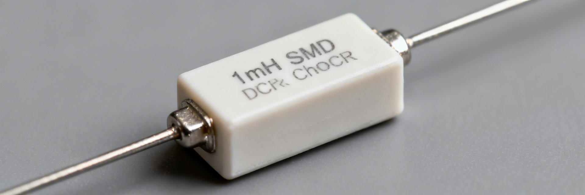
The 784777102 is a shielded, wirewound SMD/chip-style inductor optimized for low-frequency filtering and small-signal choke duties where modest inductance and compact size are needed. Its combination of 1 mH inductance and relatively high DCR positions it more for EMI suppression and filtering in low-current rails than high-efficiency power conversion. Designers should inspect test frequency and measurement voltage on the datasheet, since L and DCR are often specified at 1 kHz and a low excitation level.
Quick spec snapshot
| Parameter | Value / Notes |
|---|---|
| Part number | 784777102 |
| Inductance (nominal) | 1.00 mH |
| Rated current | ≤250 mA |
| Max DCR | ~5.75 Ω |
| Package / Type | Shielded wirewound drum, SMD |
Professional Comparison: 784777102 vs. Industry Alternatives
| Feature | 784777102 (Shielded) | Generic Unshielded | High-Current Ferrite |
|---|---|---|---|
| EMI Shielding | Excellent (Internal) | Poor (Stray Fields) | Moderate |
| DCR (Resistance) | ~5.75 Ω | ~4.5 Ω | <1.0 Ω |
| Main Application | Precision Filtering | Low-Cost Decoupling | Power Conversion |
Datasheet key electrical specs — deep analysis
Interpreting the inductor specs requires attention to stated measurement conditions, inductance tolerance, and how L changes under DC bias. Datasheets typically show L at a specified frequency and excitation; for wirewound parts, inductance can decrease with applied DC current as the core approaches saturation. Always map the datasheet’s test frequency to your intended operating band.
"When working with the 784777102, don't just look at the 1mH nominal value. In high-density layouts, the 5.75 Ω DCR is your friend for damping high-Q resonances in EMI filters, but it's your enemy for thermal budget. Pro Tip: Use 4-wire Kelvin sensing if you're verifying DCR on the bench to avoid test lead error, which can easily be 0.5 Ω."
Inductor specs breakdown
Inductance tolerance and measurement points are the first items to confirm. DCR is critical: if listed as typical vs. maximum, use the maximum for worst-case power-loss calculations. Example: with DCR = 5.75 Ω and I = 0.2 A, power loss P = I²R = 0.04 A² × 5.75 Ω = 0.23 W. That level of dissipation on a small SMD choke will produce measurable temperature rise—verify with thermal testing. Use the phrase inductor specs when comparing to alternatives and when documenting design trade-offs.
Measurement & verification: test conditions
Hand-drawn schematic, not a precise circuit diagram
Datasheets often specify ambient temperature, humidity, and the exact test fixture or lead configuration used for measurements. Matching those conditions improves reproducibility; otherwise, fixture impedance and stray inductance/capacitance can distort L and Z readings. Note whether the datasheet lists DCR under a specific temperature (e.g., 25°C) and whether reflow-affected measurements are indicated.
Practical bench tests to confirm electrical details
- L vs. Frequency Sweep: Use an LCR meter at 100Hz, 1kHz, and 10kHz to ensure stability.
- Kelvin DCR Check: Measure resistance directly at the component pads to bypass lead resistance.
- DC Bias Test: Record L drop as you approach 250mA to identify the saturation knee.
Real-world example: EMI/thermal implications
Example: input EMI choke on a 5 V rail carrying 200 mA DC. With DCR ≈5.75 Ω, the voltage drop V = I×R = 0.2 A × 5.75 Ω = 1.15 V, which is unacceptable for a 5 V rail. Power loss is ~0.23 W, likely raising the part 20–40°C above ambient on a small copper area. The tradeoff is clear: high DCR reduces EMI resonance but costs efficiency, so this part suits low-current filtering rather than supply regulation in efficiency-sensitive circuits.
Common Layout Pitfalls
- Thermal Bottleneck: Placing the 784777102 near a high-heat LDO without sufficient copper pours can lead to thermal runaway.
- EMI Leakage: Routing a digital clock line directly under the inductor. Even shielded parts have some leakage; keep a 2mm keep-out zone.
Selection checklist & integration
- Confirm inductance and tolerance meet the filter requirement (verify at 1kHz).
- Check DCR (use max value) against the power budget and voltage drop headroom.
- Ensure Rated Current ≥ 1.25× Steady-state Current for safety margin.
- Verify mechanical footprint and RoHS compliance for target manufacturing.
Summary
- Check the 784777102 datasheet for 1.00 mH nominal inductance and confirm test frequency.
- Use the max DCR (~5.75 Ω) for worst-case I²R loss; high DCR favors damping over efficiency.
- Perform bench checks: L vs. frequency and precise Kelvin DCR measurement.
CTA: Run the three bench checks listed in the Measurement section before finalizing your PCB layout.
Frequently Asked Questions
Use the maximum DCR for P = I²R calculations. At 200mA, dissipation is ~0.23W. Ensure your thermal design can dissipate this to avoid overheating nearby components.
Characterize L vs. DC Bias first. Knowing the current level where inductance drops by 10-20% is vital for maintaining filter performance during transients.


