
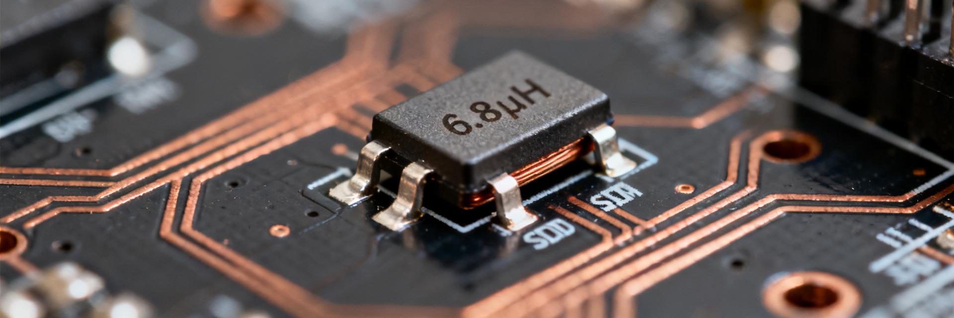
Point: This SMD power inductor targets compact power rails where space, moderate current, and mid‑frequency behavior matter. Evidence: The part is specified as 6.8 μH, ~1.54 A rated current, ~131 mΩ DCR, SRF ≈ 35 MHz in a 4.5 × 4 × 3.2 mm package (–40°C to +125°C). Explanation: Those specs define efficiency (I²R loss), ripple control (L value), and usable frequency range (SRF), making it a practical SMD power inductor for many point‑of‑load designs.
Point: The article goal is to present a datasheet‑style, testable breakdown. Evidence: Each section covers quick specs, electrical behavior, test methods, PCB/thermal guidance, and application checks. Explanation: Engineers can use this as a compact reference to evaluate 784773068 for prototyping and qualification without paging through raw PDFs.
1 — Product Overview & Quick Specs (background)
1.1 Quick spec snapshot (what to list)
Point: A concise specs table clarifies selection decisions. Evidence: Key fields include inductance, tolerance, rated current, DCR, SRF, core material, package, temperature range, mounting type, and life/MTBF. Explanation: These fields map directly to electrical, thermal, mechanical, and reliability constraints engineers check before committing to a part.
| Parameter | Typical Value |
|---|---|
| Inductance | 6.8 μH |
| Tolerance | ±20% (typical) |
| Rated Current (Isat / Irms) | ~1.54 A |
| DCR | ~131 mΩ |
| Self‑Resonant Frequency (SRF) | ~35 MHz |
| Core Material | Ferrite (powdered/ferrite composite) |
| Package | 4.5 × 4 × 3.2 mm, SMD |
| Temp Range | −40°C to +125°C |
| Mounting | SMD |
| Life/MTBF | Not specified (use standard screening) |
1.2 Who should consider this part and why
Point: Target applications include point‑of‑load buck converters, small DC‑DC modules, and EMI input filters. Evidence: The 6.8 μH value and 1.54 A rating fit moderate current regulation and mid‑frequency switching (100 kHz–2 MHz) where footprint matters. Explanation: Designers constrained by board area who accept modest conduction loss will find 784773068 useful; it’s not intended for very high‑current (>5 A) or GHz‑range RF filtering beyond its SRF.
2 — Electrical Characteristics: Detailed Specs & Their Design Impact (data analysis)
2.1 Inductance, tolerance, DCR and current ratings — practical meaning
Point: Inductance and DCR dictate ripple and conduction loss. Evidence: At 6.8 μH and ~131 mΩ DCR, I²R loss at rated current is P≈I²R = (1.54 A)²×0.131 Ω ≈ 0.31 W. Explanation: That ~0.3 W heat at 1.54 A requires thermal planning; tolerance (±20%) shifts effective L and ripple, so designers should budget margin and consider derating for saturation. Use the I²R formula and derate if measured L drops significantly near operating current.
2.2 Frequency behavior: SRF, impedance & EMI relevance
Point: SRF limits useful inductance at high frequency and defines EMI behavior. Evidence: A SRF near 35 MHz means above that frequency the part becomes capacitive and loses energy‑storage behavior. Explanation: For switching frequencies well below SRF (e.g., ≤2 MHz), the 6.8 μH is effective for energy storage; for EMI suppression in the tens of MHz the impedance peak matters — treat the part as an EMI choke only within the frequency band where its impedance rises, and avoid expecting inductive behavior past SRF.
3 — Performance Data & Test Recommendations (data analysis / method)
3.1 Typical measurements to request/perform
Point: A defined test matrix ensures part suitability. Evidence: Essential tests are L vs. frequency, DCR (4‑wire) at controlled temperature, saturation current (L vs. DC bias), thermal rise under DC, impedance vs. frequency, and solder reflow/thermal shock. Explanation: Use an LCR meter with fixture for frequency sweep, a micro‑ohmmeter for DCR, and a programmable DC source plus flux sensor/thermocouple for thermal rise. Specify pass criteria such as ≤20% L drop at rated DC bias and DCR within tolerance.
3.2 Interpreting lab data for real designs
Point: Measured curves convert to derating and safety margins. Evidence: If L drops >20% at operating DC bias or DCR is higher than spec, expected ripple and loss increase proportionally. Explanation: Translate L vs. I curves into maximum usable current (keep operating point below saturation knee), and apply a derating rule (e.g., limit continuous current to 70–80% of saturation current) to maintain inductance margin and limit thermal rise.
4 — PCB Layout, Mounting & Thermal Considerations (method guide)
4.1 Recommended footprint, soldering and assembly tips
Point: Proper land pattern and reflow yield reliable solder joints. Evidence: The part’s 4.5 × 4 × 3.2 mm body benefits from slightly oversized pads, 0.1–0.2 mm fillet allowance, and solder mask defined pads for alignment. Explanation: Use manufacturer land pattern if available; follow standard Pb‑free reflow profiles (peak ~245°C) with controlled ramp to avoid mechanical stress. Minimize mechanical strain by avoiding tight clamps during assembly.
4.2 Thermal management and reliability best practices
Point: Conduction losses create hotspots that must be mitigated. Evidence: A ~0.31 W loss at rated current concentrates heat in a small SMD package and adjacent PCB copper. Explanation: Use thermal reliefs: copper pours tied to pads, thermal vias under/near component to inner layers, and place heat‑sensitive parts away from the inductor. Observe operating temperature range and apply moisture sensitivity level (MSL) handling per standard reflow storage practices.
5 — Use Cases, Comparisons & Troubleshooting (case & action)
5.1 Typical application examples and selection checklist
Point: Two numeric examples show practical fit.
Evidence:
Example A: 5 V → 1.2 V buck at 1.5 A, fSW=500 kHz: D≈0.24, ΔIL≈(Vin−Vout)·D/(L·f) ≈ (3.8·0.24)/(6.8e‑6·500e3) ≈0.27 A peak‑to‑peak; I²R loss ≈0.31 W.
Example B: input EMI LC with cutoff ~1 MHz uses inductance and SRF to shape impedance.
Explanation: Checklist: inductance match, current margin (≥25–30% over operating current), SRF above or below intended band depending on role, package fit, and measured DCR within specs — confirm 784773068 against each item before prototyping.
5.2 Common failure modes and replacement criteria
Point: Recognizing symptoms avoids board respins. Evidence: Symptoms include overheating, rising ripple, audible noise, or open/high DCR readings after thermal cycling or shock. Explanation: Troubleshoot by measuring DCR and L, inspecting solder joints and mechanical cracks. Replace when DCR increases >20% or L falls beyond tolerance under operating bias; consider higher‑current, lower‑DCR alternatives if saturation or thermal limits are the root cause.
Summary
- 6.8 μH, ~1.54 A, ~131 mΩ and SRF ≈ 35 MHz define the 784773068 as a compact SMD power inductor for moderate current, space‑constrained power conversion; check specs against thermal and ripple budgets before selection.
- Measure L vs. frequency, DCR, saturation knee, and thermal rise in the target board; use measured curves to derate current and confirm acceptable I²R losses in the intended application.
- Follow recommended footprint, soldering, and thermal mitigation (copper pours, vias) to manage ~0.3 W typical loss at rated current and ensure long‑term reliability in prototypes and production.
Frequently Asked Questions
Is the 784773068 suitable as a general‑purpose SMD power inductor for 1–2 A buck converters?
Point: Yes for many designs. Evidence: The 6.8 μH inductance and ~1.54 A rating yield reasonable ripple control and acceptable conduction loss (~0.31 W at rated current) for 1–2 A rails when thermal layout is applied. Explanation: Ensure your switching frequency is well below the SRF and that you provide ≥25–30% current margin to avoid saturation and excessive temperature rise.
What tests should I run on 784773068 before approving a production BOM?
Point: A minimal qualification suite shortens risk. Evidence: Run L vs. frequency (including DC bias), 4‑wire DCR at board temp, saturation current, thermal rise under continuous DC, and solder reflow reliability. Explanation: Define pass thresholds (e.g., ≤20% L drop at operating bias, DCR within tolerance) and screen a representative batch to catch manufacturing variation before sign‑off.
How do I decide to replace 784773068 with a lower DCR or higher current part?
Point: Replacement is driven by thermal, ripple, or saturation limits. Evidence: If measured I²R loss causes board temps or component temps above acceptable limits, or L collapses under DC bias at operating current, select a part with lower DCR or higher Isat. Explanation: Validate replacements by repeating the same lab tests and PCB thermal checks to confirm the new part reduces loss and maintains needed inductance under bias.


