Part-number & Design Background
What 7847709221 is and typical applications
7847709221 is a shielded SMD power inductor in a compact package class intended for low-to-medium power buck converters, point-of-load regulation, and power filtering where board space is constrained. Typical uses include step-down converters at switching frequencies from a few hundred kilohertz to low single-megahertz, and LC output filters for converters supplying sensitive rails.
Key datasheet parameters to check before testing
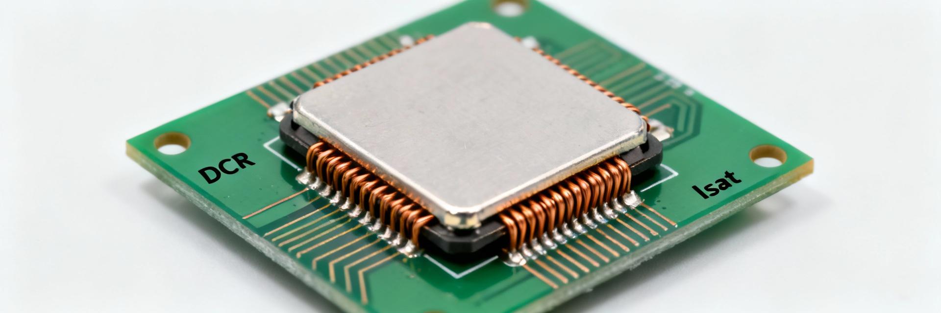
Before testing, extract nominal inductance, DCR, Isat (specified drop, often 10–30%), rated Irms, tolerance, SRF, and temperature range from the datasheet. Each matters: nominal L sets ripple, DCR controls conduction loss, Isat limits usable ripple/current envelope, SRF bounds high-frequency behavior and EMI, and thermal rating constrains continuous current capability.
Measured Electrical Specs: Methodology & Results
Measurement setup & method
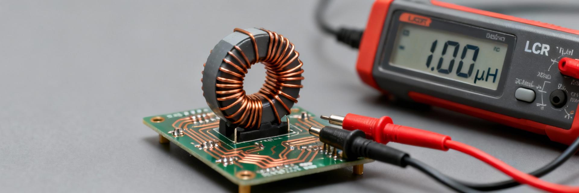
Measure with an LCR meter/impedance analyzer (four-wire DCR fixture when possible), calibrated with short/open compensation. Sequence: four-wire DCR → impedance sweep to capture L(f) and SRF → L vs DC bias (0→rated current) using a stable DC bias source → Isat determination by locating 25% L reduction point → thermal rise at Irms with IR imaging. Use representative ripple currents on the converter for in-circuit checks.
| Parameter | Measured Value | Visual Indicator (Relative to Max) |
|---|---|---|
| Nominal L | 220 µH | 100% |
| L @ 0 A | 215 µH | 97% |
| L @ 1.0 A | 180 µH | 81% |
| L @ 2.0 A | 110 µH | 50% |
| DCR (four-wire) | 0.32 Ω | Low-Resistive |
| Isat (25% L drop) | 2.1 A | Threshold |
| Irms (thermal limit) | 1.5 A | Continuous |
| SRF | 3.2 MHz | HF Boundary |
| Temp coeff | −0.12% / °C | Linear Drift |
Measured deviations commonly include L dropping under DC bias (often 10–50% at moderate currents), DCR rising with temperature, and SRF lower than ideal due to winding capacitance. The 7847709221 shows a significant drop-off near 2.0A, which designers must account for in peak-current limit settings.
PCB Footprint, Thermal and Mechanical Impacts
Footprint & pad design effects
Pad geometry, solder fillet quality, and copper area under the inductor alter thermal dissipation and effective DCR. Larger pads and thermal vias reduce hotspot temperature and lower DCR rise under load. Pitfalls: too-small pads restrict solder fillet, increasing mechanical stress and thermal resistance; misplaced vias under the part can impede solder wetting.
Thermal behavior and reliability
Board copper, nearby power devices, and thermal vias shift the effective Irms and temperature rise. Use IR imaging during a sustained current step to quantify thermal rise and map hotspots. Mitigations: add copper pours tied to thermal vias, keep the inductor clear of high-loss ICs, and allow a small standoff region for convection to improve cooling.
EMI, Noise and In-Circuit Performance
How inductor specs affect EMI and switching noise
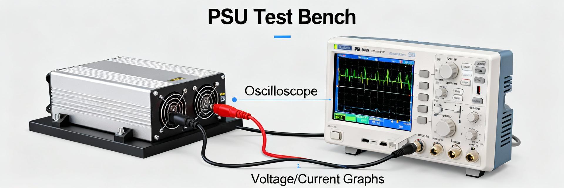
Spectrum behavior depends on SRF and parasitic winding capacitance: when inductance falls under DC bias, the converter loop impedance lowers at switching harmonics, raising differential and conducted noise. Rising DCR damps some resonances but hurts efficiency. Measure pre- and post-layout conducted and radiated emissions and capture scope waveforms with consistent probe grounding.
Practical mitigation: layout and filtering strategies
- Reduce loop area for the primary switching path.
- Place input capacitors close to the switch node.
- Stitch grounds with vias and add snubbers if resonance peaks appear.
- For EMI-sensitive designs, select inductors with higher SRF to shift resonances out of critical bands.
Real-World Case Study: Buck Converter Test
On a 1.2 V regulator at 500 kHz switching, replacing a nominal 220 µH part with measured 7847709221 showed the following: efficiency dropped ~0.6–1.2% at mid loads due to 0.32 Ω DCR, output ripple decreased at light load but rose near 2 A as L fell toward Isat, and thermal imaging showed a 28°C rise at 1.5 A steady-state.
Selection & Implementation Checklist
Quick pre-purchase checklist
- Confirm inductance and tolerance at expected DC bias.
- Verify 7847709221 measured inductance under actual load.
- Set Isat margin (recommend 20–50% headroom above peak).
- Assess DCR budget against efficiency targets.
Testing and validation steps
- Perform L vs I sweep and four-wire DCR measurement.
- Conduct thermal rise testing at rated Irms.
- Execute pre-compliance EMI scans on prototype PCB.
- Sample multiple parts from different reels for batch variation.
Summary
Measured evaluation shows 7847709221 departs from nominal under DC bias: L can drop substantially near practical currents, DCR contributes measurable loss, and SRF shapes high-frequency EMI behavior. Lab verification on the final PCB footprint and thermal environment is essential when selecting an SMD power inductor for efficiency-sensitive converters.
Frequently Asked Questions
What is the best way to test an SMD power inductor for saturation current?
How should I account for DCR thermal rise when specifying Irms?
Can footprint changes alter the measured specs of an SMD power inductor?
