
Recent bench work and supplier datasheets show consistent trade-offs for compact 1 mH shielded SMD inductors: substantial inductance roll‑off under DC bias, measurable DCR and thermal losses that cap RMS current, and self‑resonant frequencies (SRF) that limit high‑frequency blocking. This piece compiles key metrics, test methods, and practical picks for US hardware teams focused on power filtering, EMI suppression, and low‑frequency decoupling.
Engineers will find concise selection heuristics, a hands‑on measurement checklist, and application profiles that translate performance data into procurement criteria. Recommendations emphasize measurable margins (Isat/Irms), DCR thermal effects, and SRF placement relative to target frequencies, with explicit in‑circuit validation steps for production acceptance.
(Background) — What is a 1 mH shielded SMD inductor and when to use it
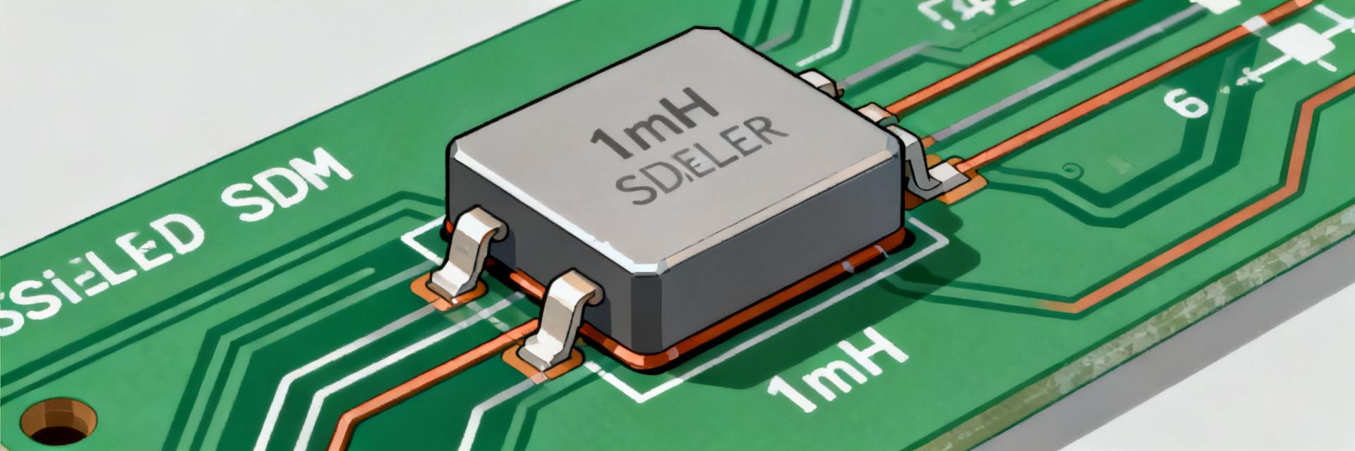
A 1 mH shielded SMD inductor is a surface‑mount magnetic component delivering roughly 1 millihenry of inductance in a compact, shielded package. Use it where board area and automated assembly are priorities but magnetic coupling or EMI leakage must be minimized—dense RF environments, mixed‑signal boards, and compact power filters benefit most from shielding.
Design & shielding benefits
Shielded SMD construction typically combines a magnetic core and a plated metal shield or closed magnetic path to contain flux and reduce coupling. Shielding lowers radiated EMI and eases placement near sensitive analog blocks. The trade‑offs are slightly higher DCR and sometimes larger height; layout should keep return paths short and avoid routing loops beneath the part.
Typical electrical & mechanical specs to expect
| Parameter | Typical Range / Value |
|---|---|
| Inductance | 1 mH ± tolerance |
| DCR | Few ohms to sub-ohm |
| Isat (Saturation) | 0.2 – 5 A |
| SRF | Low MHz band |
(Data analysis) — Performance data: how these inductors behave under test
Meaningful performance data comes from standardized sweeps: L vs frequency, L vs DC bias, DCR vs temperature, SRF, and thermal rise under load. Consistent test methods let teams compare parts on equal footing. Below are recommended measurements and interpretation rules for bench validation and supplier data cross‑checks.
Test methods & measurement setup
Use Kelvin DCR fixturing, open‑short compensation for L‑meter sweeps, and a vector network analyzer or precision LCR for SRF. Recommended plots: L(f) from 100 Hz to several MHz, L(I) to rated DC bias, DCR(T) from ambient to operating temps.
Performance curves to interpret
Essential plots: inductance vs frequency (shows roll‑off toward SRF), inductance vs DC bias (percent L drop at Irms and Isat), DCR vs temperature, and insertion loss for EMI filter topologies.
(Comparative analysis) — Shielded SMD vs other inductor options
Shielded SMD choices sit between unshielded SMD and larger wire‑wound through‑hole parts. Trade‑offs include EMI containment, footprint and height, DCR, cost, and thermal behavior.
(Selection guide) — Choosing the right inductor for your design
Electrical selection checklist
- L vs DC bias: Acceptable percentage drop (typically
- Isat Margin: Use Isat ≥1.5× peak DC for switching.
- Irms Margin: Irms ≥1.25× thermal steady‑state current.
- DCR: Maximum allowable and expected thermal rise.
- SRF: Comfortably above or below application band.
Mechanical & Reliability
Check footprint and height limits, solder fillet guidance, and reflow profile compatibility. Specify shock, vibration, and thermal cycling tests for critical designs. Recommend sample thermal cycling and solderability checks post-reflow.
(Picks & procurement) — Recommended picks by application
High-Current Filter
DCR ≤0.5 Ω, Isat ≥2× peak, SRF >10× switching freq.
EMI Suppression
Tight shielding, DCR ≤1 Ω, SRF tuned to interfering band.
LF Decoupling
Stable L under DC bias, L drop ≤30% at expected load.
Summary
For US engineering teams selecting a 1 mH shielded SMD inductor, prioritize measured performance—L vs DC bias, DCR/thermal limits, Isat/Irms margins, and SRF—and validate with the bench tests and supplier data outlined above.
- Measure L vs DC bias and L vs frequency to see real operating inductance; use parts with ≤30% L drop at expected DC bias.
- Use DCR vs temperature and thermal rise tests to set Irms limits; apply Isat ≥1.5× peak DC and Irms ≥1.25× steady current.
- Select SRF relative to the application: SRF well above switching harmonics or below interfering bands for EMI suppression.
Frequently asked questions (FAQ)
What test data should I request for a 1 mH shielded SMD inductor?
Request L vs frequency, L vs DC bias (to rated current and Isat), DCR vs temperature, SRF, thermal rise under specific Irms, recommended land pattern, and reflow profile.
How much inductance drop under DC bias is acceptable?
For power‑filtering and decoupling, target ≤30% inductance reduction at expected DC bias; aggressive applications may accept up to 50% if compensated in circuit.
How should I validate batches of 1 mH shielded SMD inductors in production?
Implement automated DCR and L spot checks on a statistical sample per lot, confirm reflowed samples retain inductance within tolerance, and perform thermal‑rise spot tests.


