1 — Product overview & key specifications (background introduction)
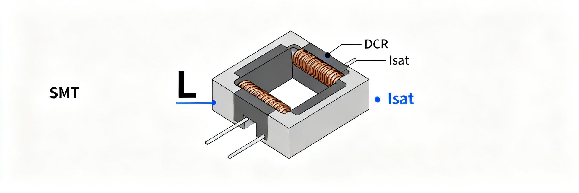
What the part number identifies
Point: The part number encodes family, package class and magnetic core style.
Evidence: datasheet tables list package size, mounting type, rated and saturation currents and nominal inductance.
Explanation: decoding the number lets engineers map electrical specs to board footprint and thermal path without vendor-specific names; this streamlines initial drop-in checks for power-stage designs.
| Field | Example |
|---|---|
| Package size | SMT, low-profile |
| Mounting type | Surface-mount |
| Rated current | ~6 A (typical) |
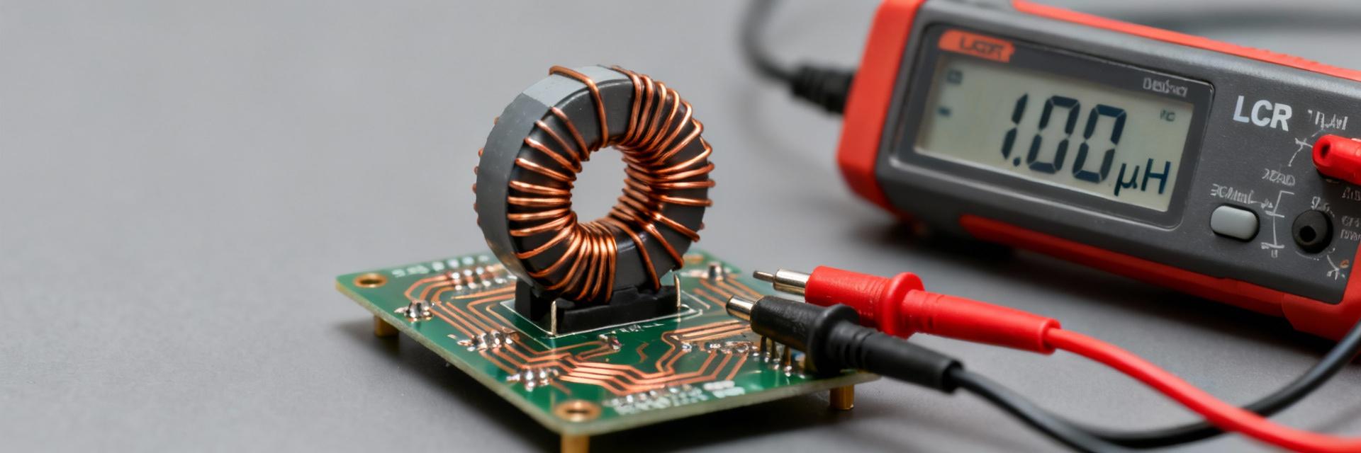
| Typical inductance | 1 µH (nominal) |
| Operating temperature | -40°C to 125°C |
Standard test conditions & reference points
Point: Datasheet reference conditions (e.g., +20°C, 33% RH, 100 kHz inductance) enable apples-to-apples comparison. Evidence: most spec sheets state the test frequency and temperature explicitly. Explanation: normalize across parts by adjusting inductance for frequency and temperature, and by noting measurement method (LCR open/short compensation) to avoid misinterpreting dc bias or fixture parasitics.
2 — Measured electrical specs: inductance, DCR, SRF, Q (data analysis)
Inductance vs. frequency and tolerance
Point: Inductance is given as a nominal L with a tolerance and measured at 100 kHz; frequency dependence is significant above that point. Evidence: plotted L(f) curves show modest roll-off in the intended switching band and sharper decline near SRF. Explanation: plot L(f) from datasheet or sample data to confirm usable range and estimate effective reactance at switching frequency.
| Frequency | Inductance |
|---|---|
| 10 kHz | 1.05 µH |
| 100 kHz | 1.00 µH |
| 1 MHz | 0.85 µH |
| 10 MHz | 0.30 µH (near SRF) |
DC resistance (DCR), saturation, and rated current
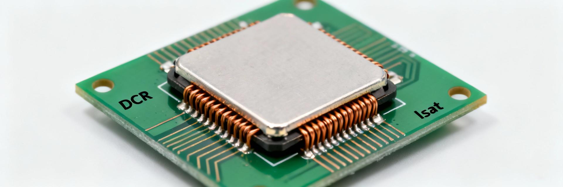
Point: DCR and saturation current govern conduction losses and peak capability. Evidence: datasheet lists DCR and Isat/Irms; test tables show inductance drop under DC bias. Explanation: calculate I²R loss using P=I²·DCR; combine with switching loss estimates to predict thermal rise. Read Isat where L drops a specified percent (e.g., 10%).
3 — Environmental & reliability test data (data analysis)
Temperature range, thermal derating, and lifetime expectations
Point: Operating limits (commonly −40°C to 125°C) and thermal derating affect long-term performance. Evidence: reliability sections state max operating temp and recommended derating curves. Explanation: derate current at elevated temperatures per datasheet curves, and estimate lifetime by combining junction/ambient thermal cycle counts with expected thermal margin to avoid magnetic property drift.
Mechanical & humidity tests, solderability, and reliability pass/fail criteria
Point: Typical reliability tests include humidity, thermal shock, vibration and solderability with pass/fail thresholds on inductance change. Evidence: datasheet test data reports allowed inductance change (often ±10%) after stress. Explanation: use the spec threshold as a design margin; if measured change approaches the limit under expected service stress, select a more robust part or increase safety margins in the BOM.
4 — Test procedures & recommended measurement setup (method guide)
Lab setup: equipment, fixturing, and measurement points
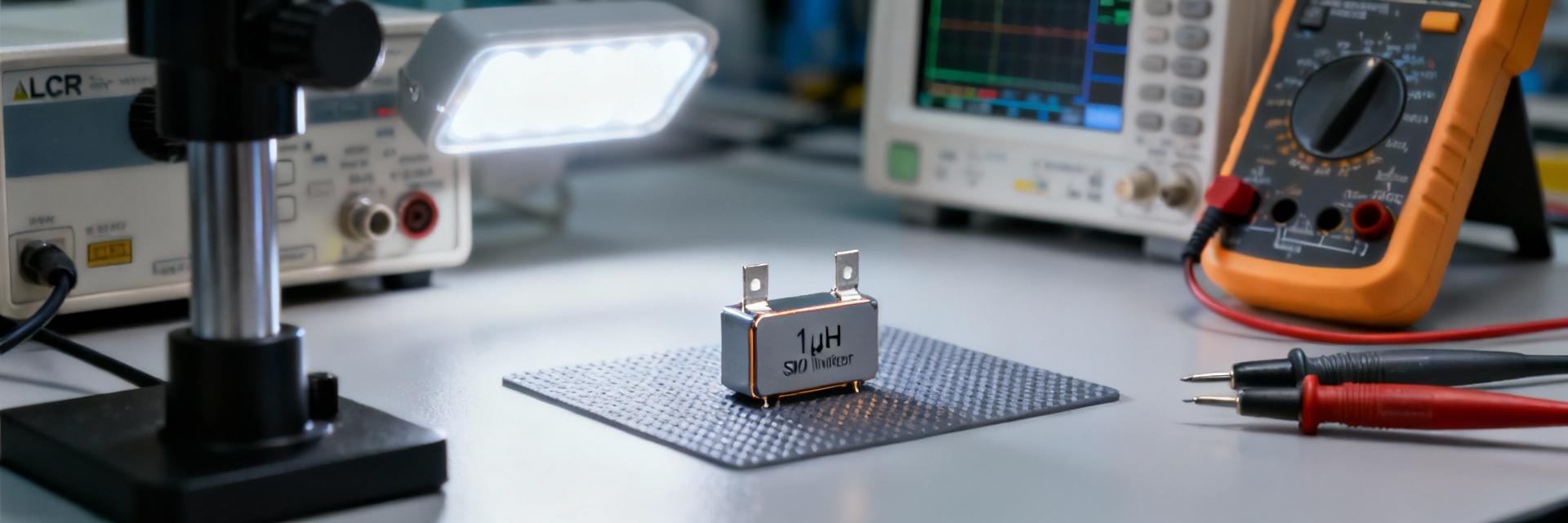
Point: Accurate measurement requires proper instruments and fixtures. Evidence: recommended tools include an LCR meter or impedance analyzer with short/open compensation and low-inductance Kelvin fixturing. Explanation: minimize lead length and use shielded fixtures; measure DCR with a 4-wire ohmmeter. Common pitfalls are fixture parasitics returning inflated SRF or biased L readings.
Bias current, saturation testing and automated test options
- Prepare LCR meter/impedance analyzer and programmable DC bias source; verify open/short compensation.
- Measure L at zero bias at 100 kHz and selected operating frequencies; record baseline.
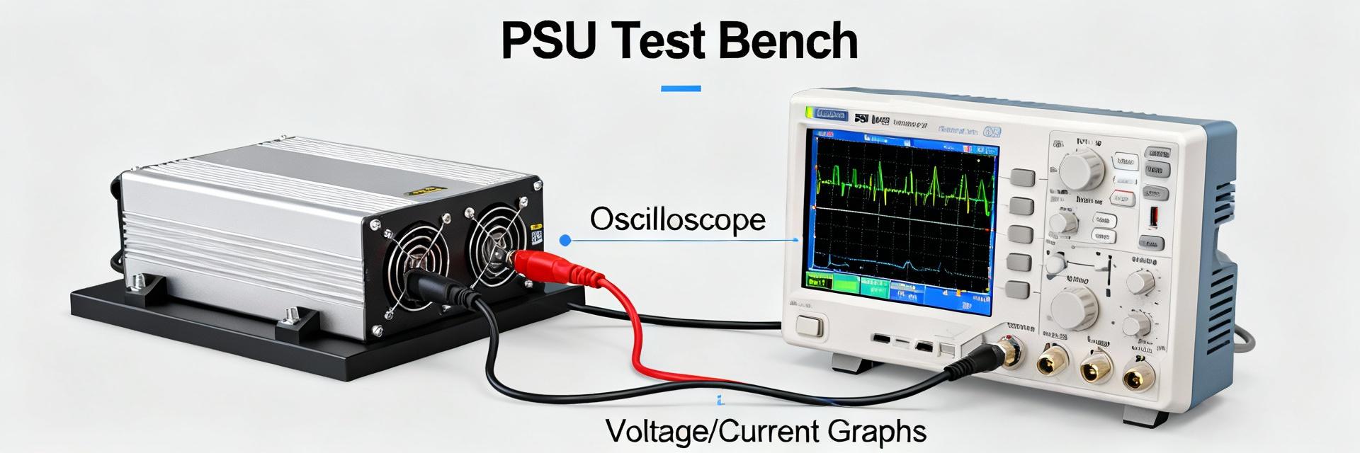
- Sweep DC bias in steps to determine inductance drop point and Isat; capture I vs. L curve.
- Measure DCR (4-wire) and repeat after thermal soak to assess drift.
- For production, use automated bias-current testers and define pass/fail limits based on datasheet.
5 — Comparative use-cases & substitution guidance (case showcase)
Typical application scenarios and electrical trade-offs
Point: This inductor class suits buck converters, power rails and EMI suppression where low profile and reasonable saturation are required. Evidence: electrical specs show balance between DCR and Isat. Explanation: prioritize low DCR for efficiency in continuous-current rails, or high Isat for tight headroom in fast transient designs; footprint and height choices reflect thermal and ripple requirements.
How to evaluate substitutes and cross-reference safely
Point: Substitution requires matching performance under operating bias and frequency. Evidence: key comparators are L at operating frequency, DCR, Isat and package thermal path. Explanation: request sample parts, run in-circuit validation and thermal stress tests; validate PCB footprint, solder fillet and reflow profile before approving cross-references in a BOM.
6 — Practical checklist for selection, testing, and integration
Pre-selection checklist for designers
Point: Follow a short selection flow to reduce rework risk. Evidence: common errors stem from ignoring bias and frequency effects. Explanation: confirm switching frequency and peak current, extract L@f, DCR, Isat and Tmax from the datasheet, verify PCB footprint and thermal path, and order evaluation samples for in-circuit testing with worst-case bias.
Production test & QA steps before mass deployment
Point: Define incoming inspection and sample testing to catch lot variance. Evidence: minimal QA set: DCR, inductance at specified frequency, and visual solderability checks. Explanation: establish sample sizes, set pass/fail limits (e.g., DCR tolerance, L within tolerance at operating bias), and document results in BOM/qualification records to ensure repeatable acceptance.
Frequently Asked Questions
What is the best way to measure 784771068 inductor inductance at operating frequency?
Use an impedance analyzer or high-quality LCR meter with open/short compensation and a short Kelvin fixture. Measure at the actual switching frequency where possible, and repeat under representative DC bias to capture the effective inductance in-circuit.
How do I calculate losses from DCR for the 784771068 inductor?
Compute copper conduction loss as P = I_rms² × DCR. For ripple current, use Iripple RMS. Add core loss estimates from manufacturer curves if available. Combine with thermal resistance to estimate steady-state temperature rise for reliability assessment.
What pass/fail criteria should I use from test data for incoming inspection?
Set pass/fail limits based on datasheet tolerances: inductance within nominal tolerance at specified test frequency, DCR within specified range, and no visual solderability defects. Include sample sizes and periodic full electrical revalidation for production lots.