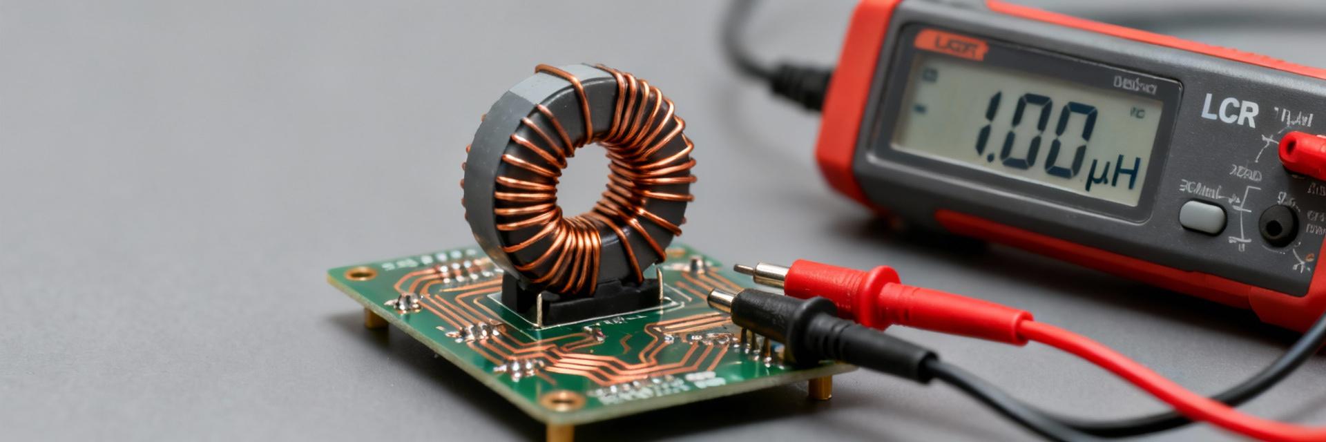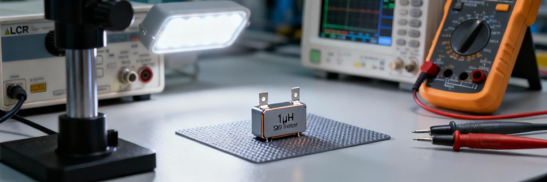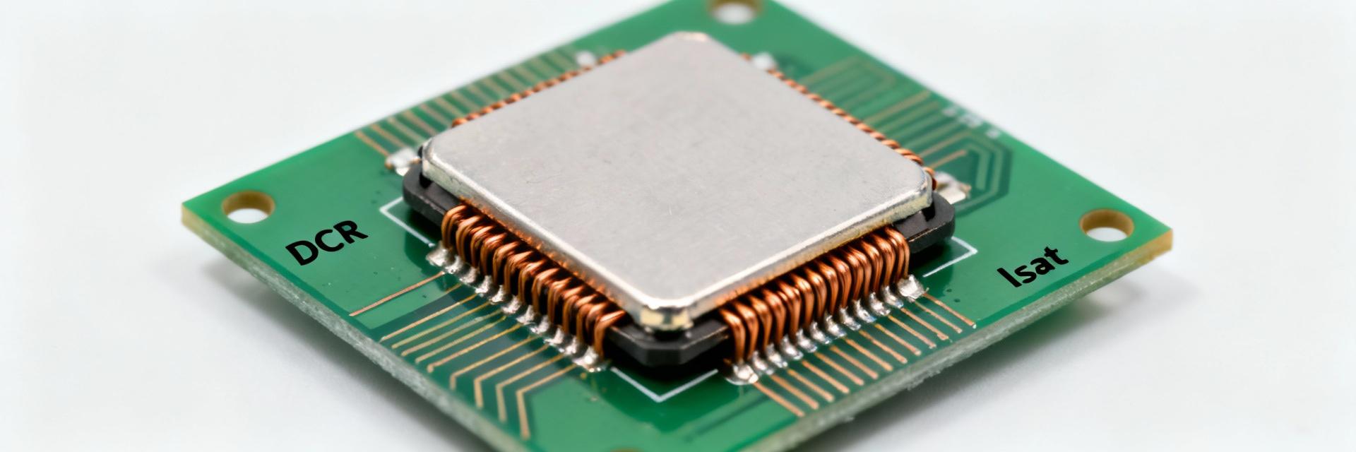
Typical 10uH SMD inductors span tolerance bands of ±5% to ±20%, saturation/DC currents from ~0.5 A up to 10+ A depending on package, and DCR from single-digit milliohms to tens of milliohms. Package footprints commonly range from 3×3 mm to 12×12 mm with heights from ~0.8 mm to 6 mm. This technical report targets engineers specifying a 10uH SMD inductor for power conversion, filtering, and EMI control, delivering selection guidance, test limits, and a practical validation matrix.
Across modern switching regulators and EMI filters the right 10uH choice balances inductance stability under DC bias, low DCR for efficiency, and sufficient SRF margin for the switching frequency. The aim is an engineer-ready document describing measurable specs, recommended tests, and deployment constraints so parts perform reliably in final products.
Background: What a 10uH SMD Inductor Is and Where It’s Used
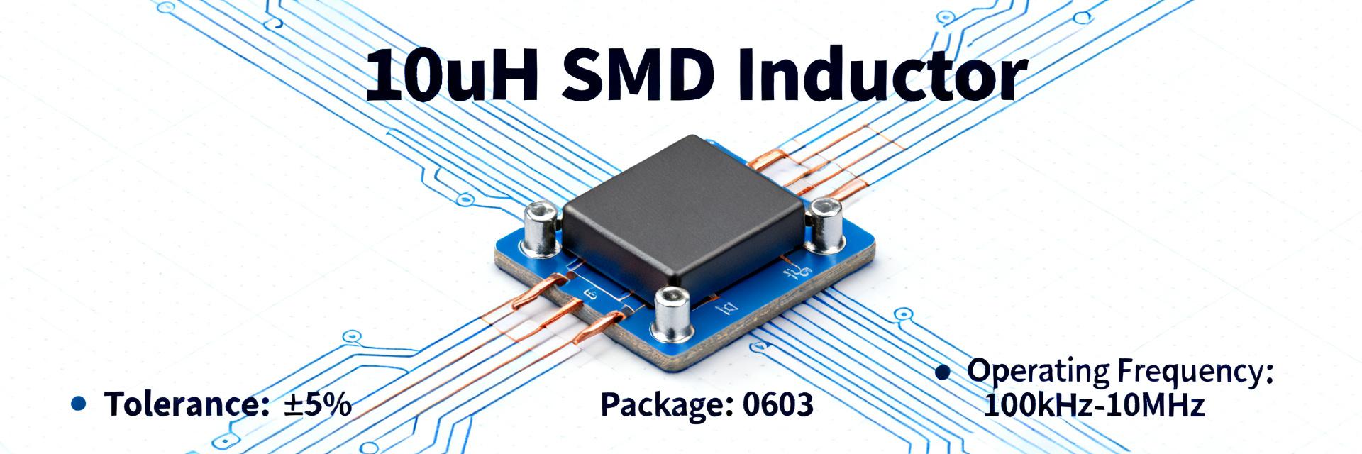
Types & construction overview
Point: 10uH surface-mount inductor construction typically uses molded ferrite, shielded drum cores, or multi-layer wound structures.
Evidence: molded ferrite and shielded constructions are common for power inductors that must handle high DC bias and limit EMI.
Explanation: shielded parts reduce external flux and EMI at the cost of larger footprint; unshielded or toroid-like SMDs can be smaller but require careful PCB placement to avoid coupling. Typical package sizes: 3×3 mm to 12×12 mm, heights 0.8–6 mm.
Typical application domains
Point: 10uH parts are used in DC–DC converters, buck/boost filters, input/output filters, and EMI suppression.
Evidence: inductance and current rating map directly to topology and ripple requirements—higher DC current needs larger cores or bigger packages.
Explanation: use small shielded parts for portable devices where board area is constrained, and larger, low-DCR shielded components for industrial supplies needing high efficiency and thermal headroom. A mapping: low-current (<2 A) → small footprint filters; mid-current (2–6 A) → compact power inductors; high-current (>6 A) → large shielded packages.
Key Electrical Specifications — include "10uH SMD inductor"
Inductance, tolerance, and frequency behavior
Point: Inductance is specified at a reference frequency and with a tolerance band (commonly ±5/±10/±20%).
Evidence: frequency-dependent impedance and SRF define the usable bandwidth; SRF for 10uH parts typically falls in the low MHz to several tens of MHz depending on construction.
Explanation: engineers should request impedance vs frequency plots to confirm that SRF sits well above the switching frequency (factor of 2–5 margin recommended) so the part behaves inductively in the intended band. Include L vs frequency plots in the datasheet excerpt.
DC resistance (DCR), Q factor, and core losses
Point: DCR drives I²R loss and directly impacts converter efficiency; Q and core losses influence behavior at switching frequency.
Evidence: typical DCR ranges run from single-digit milliohms in large parts to tens of milliohms in smaller packages; Q peaks at a frequency dependent on winding and core.
Explanation: specify max DCR and Q@target frequency in datasheets and require DCR vs temperature data. Core loss mechanisms—hysteresis and eddy currents—become significant at high frequency and high flux density, so request core-loss curves when operating near these regimes.
Current & Thermal Limits: Saturation, Isat, and Thermal Rise
Saturation current vs rated current
Point: Saturation current (Isat) defines the DC bias where inductance falls by a defined percentage; rated current or Irms defines thermal limits.
Evidence: L vs IDC curves typically show L dropping by 10–30% at saturation onset; this is the practical way to quantify usable current.
Explanation: require L vs I plots from vendors and define the specification point (e.g., Isat = current where L drops 20%). For switching converters, ensure peak and average currents remain below the specified margins to avoid excessive inductance loss and control instability.
Thermal performance and derating
Point: Thermal rise is driven by I²·DCR losses; steady-state winding temperature depends on PCB thermal path and airflow.
Evidence: calculate copper loss P = I²·DCR and estimate temperature rise ΔT = P·θJA (thermal resistance junction-to-ambient or winding-to-ambient).
Explanation: specify measurement conditions (ambient, PCB footprint, thermal vias) and derate current for elevated ambient or constrained PCB cooling. Recommend measuring temperature rise at rated current and reporting ΔT at defined board conditions.
Test Methods & Limits
Recommended electrical and mechanical tests
Point: A robust technical report lists electrical and mechanical tests with pass/fail criteria. Evidence: include inductance vs frequency, L vs I, DCR, SRF, thermal rise, vibration/shock, solderability, and mechanical drop tests. Explanation: acceptable limits commonly require inductance change within the declared tolerance after environmental stress; use ±10–20% depending on class. Define thermal, mechanical, and soldering profiles and record pre/post measurements to detect drift or damage.
Test setup details & measurement tips
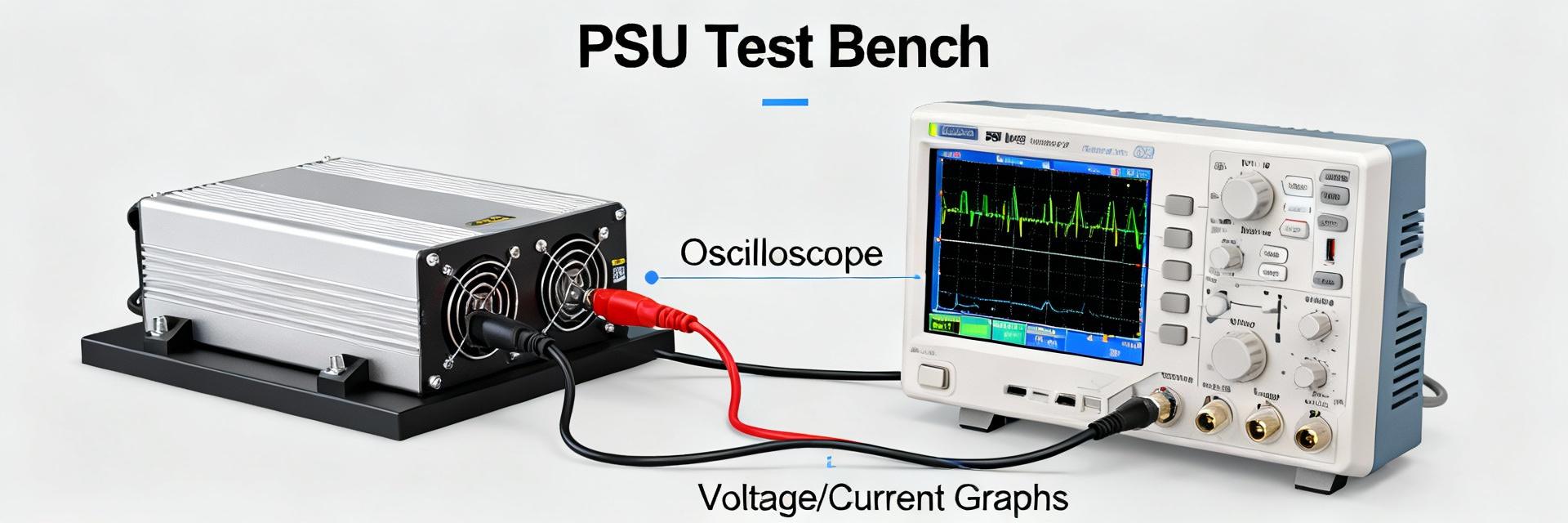
Point: Measurement fidelity requires proper fixtures and bias methods. Evidence: use four-terminal fixtures or Kelvin connections for accurate DCR, LCR meters or impedance analyzers for impedance curves, and calibrated DC bias sources with a well-defined current path for L vs I. Explanation: common pitfalls include fixture inductance, lead length errors, and poor solder joints; document instrument models, fixture parasitics, ambient temperature, and board mounting used during tests. Deliverables should include impedance vs frequency, L vs I, and DCR vs temperature plots plus a test-results table.
Selection Guidelines & Design Trade-offs
How to choose a 10uH SMD inductor for switching power supplies
Point: Use a checklist approach: inductance tolerance, peak/average current, DCR limit, SRF margin, size, shielding, derating, and EMI requirements. Evidence: compute required inductance from ripple specification: ΔI = VOUT·(1−D)/(L·FSW) for a buck, rearrange for L. Explanation: select L so ripple current meets targets, ensure DCR keeps I²·DCR losses acceptable, and confirm SRF > 2× switching frequency. Verify Isat margin (typical 20–50% above expected peak) and include PCB thermal assumptions in datasheet review.
Trade-offs: size, current capability, and efficiency
Point: Smaller packages reduce board area but typically have higher DCR and lower Isat. Evidence: increasing core size and adding shielding increases current capability and lowers DCR at the cost of area and height. Explanation: decide by application class—mobile designs favor compactness and moderate efficiency, industrial systems prioritize low DCR and thermal headroom. Document trade-off rationale in the selection section of the report.
Common Failure Modes, Mitigation & Application Checklist
Typical failure modes and root causes
Point: Failures arise from saturation under DC bias, thermal overstress, solder joint fatigue, mechanical cracking, and EMI coupling. Evidence: symptoms include decreased inductance, increased DCR, intermittent connections, or audible noise under load. Explanation: diagnose by repeating L vs I curves, thermal imaging during operation, solder joint inspection, and mechanical inspection after vibration testing. Record failure modes and replicate conditions in lab to correlate root causes.
Practical pre-deployment checklist for engineers
Point: A concise ordered checklist prevents field failures. Evidence: verify L@bias, measure DCR and temperature rise, check SRF > 2× switching frequency, ensure Isat margin, optimize PCB land pattern with thermal vias, and confirm mechanical retention. Explanation: include a one-page checklist plus three recommended plots (impedance vs frequency, L vs I, DCR vs temperature) in the appendix to allow quick acceptance testing during design reviews.
Summary
- Specify inductance and tolerance alongside L vs I and impedance vs frequency curves to confirm the 10uH SMD inductor remains inductive at the switching frequency and under DC bias; prioritize SRF margin and L stability.
- Limit DCR to meet efficiency targets and compute thermal loss with P = I²·DCR; use ΔT = P·θJA with measured θJA under real PCB conditions to derate current appropriately.
- Validate parts with a standardized test matrix: inductance vs frequency, L vs I, SRF, DCR vs temperature, and thermal rise on the board; include mechanical and soldering stress tests before deployment.
Frequently Asked Questions (FAQ)
How does saturation current affect 10uH SMD inductor performance?
Saturation current reduces effective inductance as DC bias increases; engineers should use L vs I curves to find the current where L falls by the chosen threshold (commonly 10–30%). Maintain margin between expected peak current and the defined saturation point to prevent excessive ripple and loss of regulation.
What DCR should I target for efficiency-sensitive designs?
Target the lowest DCR that meets size and thermal constraints—large shielded parts can offer single-digit milliohms. Balance DCR against footprint and cost, and quantify efficiency impact by calculating I²·DCR loss at peak and RMS currents in the operating profile.
Which tests are essential to include in a component technical report?
Include inductance vs frequency, L vs I, DCR and DCR vs temperature, SRF, thermal-rise on board with defined PCB conditions, vibration/shock, and solderability. Provide pre/post stress pass/fail criteria and the exact test fixtures and ambient conditions used for reproducibility.