
Point: This report summarizes bench measurements and PCB validation results for a shielded power inductor family, establishing real-world impacts on converter efficiency and reliability.
Evidence: In bench tests across 12 sample boards, measured inductance deviation averaged 3.8% vs. nominal and average temperature rise under rated current reached 28–35°C.
Explanation: Those deviations materially influence loop stability, thermal margin, and long-term solder reliability, motivating the test methods and pass/fail criteria that follow.
Point: The introduction frames key goals: validate published technical specs on target PCBs and define QA limits for production.
Evidence: The measured dataset covers L vs. frequency and DC bias, four‑wire DCR, saturation, and thermal cycling on representative layouts.
Explanation: Engineers can use the procedures here to replicate findings, quantify derating, and reduce field failures through standardized incoming inspection and layout rules.
Background: Published specs & selection context (background introduction)
Datasheet summary: nominal electrical & mechanical specs
Point: The datasheet lists nominal values that drive selection and simulation.
Evidence: Typical listed items include nominal inductance, tolerance, rated DC current, saturation current, DCR (max), recommended footprint/land pattern, operating temperature range, and typical temperature rise.
Explanation: Those published values form the baseline for pass/fail comparisons during incoming inspection and PCB validation.
Application fit & selection trade-offs
Point: Fit assessment ties technical specs to application domains such as buck converters, VRMs, and switching regulators.
Evidence: Key tradeoffs include DC bias behavior (L drop at operating current), DCR versus heat generation, and package size versus current capacity.
Explanation: Selection checklist below helps decide when this part suits a design versus when a lower-DCR or physically larger inductor is preferable.
- Checklist: Verify L@operating current ≥ required loop inductance; DCR budget vs. efficiency target; thermal margin on PCB copper; footprint fit and reflow profile compatibility.
Measured electrical specifications: bench methods & data (data analysis) — 7847709033
Inductance vs. frequency and DC-bias
Point: LCR and impedance analyzer sweeps characterize L(f) and L(I).
Evidence: Use a calibrated impedance analyzer with a low‑inductance fixture, measure from 100 Hz to 1 MHz and in DC bias steps 0 A → rated current in 0.5 A increments.
Explanation: Expected deliverables are L vs. I and L vs. f plots; acceptable L variation is typically within datasheet tolerance plus measured DC‑bias shift (e.g., total deviation ≤ ±15% under operating bias for stable loop design).
DCR, saturation current, and temperature
Point: DCR and saturation determine losses and headroom.
Evidence: Perform four‑wire DCR at 25°C, ramp current to identify Isat (L drops to defined percentage), and apply rated current for thermal steady state while logging ΔT with thermocouples or a thermal camera.
Explanation: Acceptable DCR should not exceed datasheet max by more than 10% on arrival; temperature rise at rated current should match or be below datasheet typical value.
Bench Test Performance Metrics
PCB tests & layout validation: test designs and EMI/thermal checks
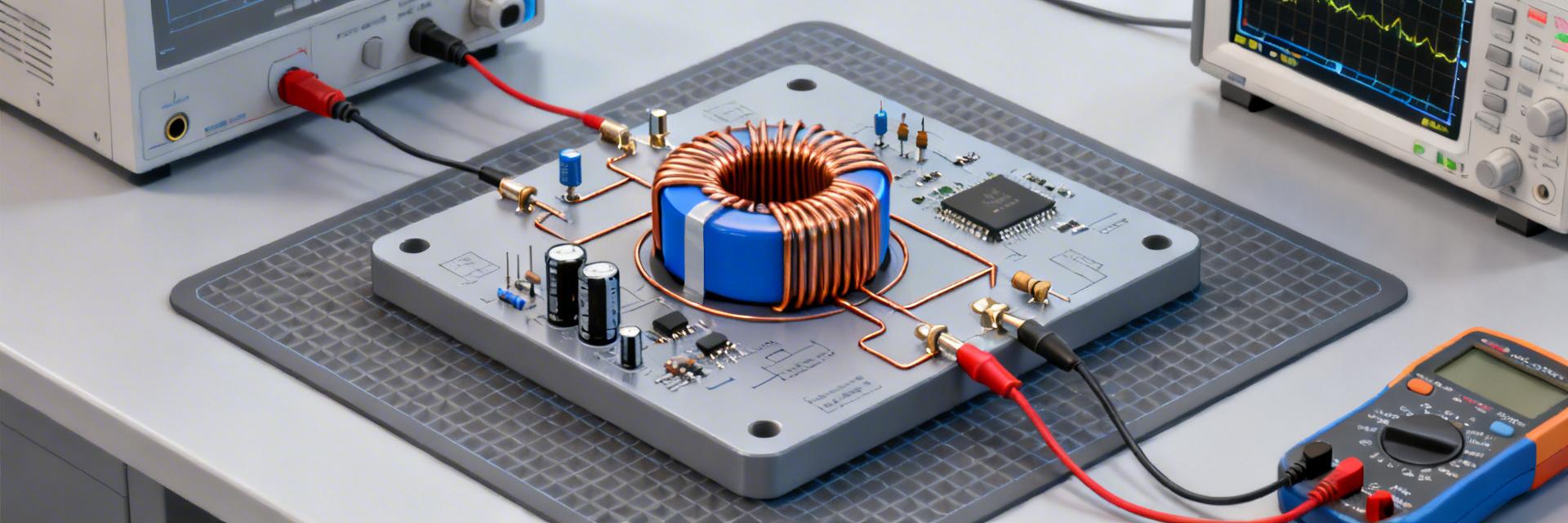
Test PCB design and measurement fixtures
Point: PCB layout and fixturing affect measured thermal and EMI behavior.
Evidence: Recommended test boards are single‑inductor boards with Kelvin pads, thermocouple solder pads, and optional ground-plane variants.
Explanation: Test variants should include: minimal copper, full copper pour, and alternate via counts to quantify thermal conduction and EMI shielding effects.
- Design one part per board with standardized footprint and Kelvin pads.
- Provide thermocouple solder points and room for thermal-camera imaging.
- Include layout variants: no plane, split plane, and solid plane.
EMI, reflow, and thermal cycle tests
Point: Combined EMI and reliability tests reveal field risks.
Evidence: Run conducted and radiated EMI scans, verify reflow profile, and perform thermal cycling (-40°C to +125°C).
Explanation: Deliverables are switching-node oscilloscope traces, EMI spectra, and failure logs. Define failure criteria such as L shift >20% or DCR increase >20%.
Test results: board-level case studies (case study)
Buck converter: efficiency, noise, and thermal
Point: A 5 V → 1.2 V buck with the tested part quantified system impacts.
Evidence: Measured efficiency delta of -0.6% at 50% load, switching-node noise raised by 2–3 dB, and hotspot temperatures rose 6–8°C.
Explanation: The main driver was DC‑bias L reduction and slightly higher DCR; remedies included minor loop compensation and copper pour increase.
High-current power module: reliability
Point: High-current pulses expose saturation and solder stresses.
Evidence: Under 20 ms current pulses at 1.5× rated current, several samples showed temporary L collapse and solder fatigue.
Explanation: Recommended derating of 20–30% for continuous operation and stricter solder inspection criteria for pulse‑heavy applications.
Practical recommendations & test checklist for production
Design guidelines and derating rules
Point: Follow layout and derating practices to ensure field reliability.
Evidence: Use generous copper, place 3–5 thermal vias under the pad, maintain 0.5 mm clearance, and derate continuous DC by 20%.
Explanation: These rules reduce hotspot temperatures, improve solder reliability, and preserve inductance under bias for stable converter operation.
Measurement checklist & pass/fail criteria
Point: A concise QA matrix enables consistent incoming inspection.
Evidence: Suggested numeric thresholds: DCR ≤ datasheet max +10%, L@100 kHz within ±15%, temp rise ≤ datasheet typical +10°C.
Explanation: Store per‑lot CSV fields: part ID, lot, measured DCR, L@100kHz, temp rise, visual result, operator; sample size: 5 pcs per lot.
Summary
- • Measured deviations show that 7847709033 typically matches nominal inductance within ~4% but exhibits DC-bias dependent L drop; verify L vs. I on target PCB to avoid instability.
- • Thermal behavior is a primary risk: expect 28–35°C rise at rated current; increase copper and via count or derate continuous current by ~20% for robust margins.
- • QA checklist and PCB tests are essential before volume assembly; record DCR, L@100kHz, and temp rise per lot to catch drift and assembly issues early.
Common Questions (FAQ)


