
Lab surveys of SMD power inductors show nominal inductance can shift by 20–30% under DC bias and thermal stress — critical if your design relies on the SPM3020T-4R7M. This analysis breaks down datasheet values versus practical, measured limits to ensure reliable power-rail performance.
1 — Product Snapshot & Typical Applications
What this part is and where it fits
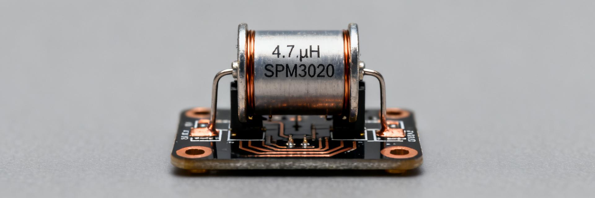
The SPM3020T-4R7M is a shielded SMD power inductor with a nominal inductance of 4.7 µH in a 3020 footprint (3.0 x 2.0 mm). It is specifically engineered for DC–DC converter applications, such as buck regulators and point-of-load (POL) power rails, where a compact profile and stable wire-wound construction are required.
| Parameter | Datasheet Value | Typical / Notes |
|---|---|---|
| Nominal L | 4.7 µH | Measured at 100kHz/1MHz (see datasheet) |
| Tolerance | ±20% | Standard manufacturing variance |
| Rated Current (Idc) | ~1.9 A | Design derate to 1.2–1.6 A recommended |
| DCR (Max) | ~0.08–0.12 Ω | Critical for I²R efficiency calculations |
| Dimensions | 3.0 × 2.0 × 2.0 mm | 3020 Metric / 1208 Imperial |
2 — Key Specs Extracted from Datasheet
Electrical Performance Analysis
Inductance is quoted under small-signal conditions. However, under real-world DC bias, the effective L will drop. Designers should utilize the datasheet’s ΔL curves to determine the actual inductance at their operating current. The Idc rating is typically constrained by a 40°C temperature rise or a specific percentage drop in inductance (Saturation).
| Electrical Metric | Value | Condition |
|---|---|---|
| Inductance | 4.7 µH | Initial @ 0A DC |
| Isat (Typ) | ~2.1 A | L drops by 30% |
| Temp Rise Current | ~1.9 A | ΔT = 40K rise |
| Operating Temp | -40 to +125°C | Including self-heating |
3 — Measured Limits: Lab Tests You Should Run
Typical Measured Variation
Bench tests often reveal that wire-wound components like the SPM3020T-4R7M exhibit a 20–30% reduction in inductance when approaching the rated Idc. Furthermore, DCR increases as the component heats up, following the copper temperature coefficient (~0.4%/°C). To ensure stability, perform an impedance sweep and log results to a CSV for design records.
4 — Design Implications & PCB Guidelines
Thermal and EMI Strategy
- Placement: Position the inductor as close to the switch node as possible to minimize EMI loop area.
- Copper Pours: Use large copper areas and thermal vias to dissipate heat from the pads.
- Keep-out Zones: Avoid routing sensitive analog traces directly under the inductor to prevent magnetic coupling.
5 — Troubleshooting Common Failure Modes
If you experience excessive heating or voltage ripple, inspect the solder joints and re-verify the saturation current. Mitigation involves selecting higher-Isat variants or improving airflow. Always document "Measured L vs Idc" curves to provide procurement with objective substitution criteria.
Summary
Before committing the SPM3020T-4R7M to mass production, verify its performance under your specific thermal and current constraints. Datasheet values provide a baseline, but measured limits dictate real-world reliability.
- Calculate I²R losses based on DCR at operating temperature.
- Assume a 20-30% L reduction at peak load.
- Apply a 20% current derating for high-ambient environments.
Industry FAQ
How should I validate the SPM3020T-4R7M for my design?
Run L vs Idc, DCR at temperature, and a temperature-rise test under expected continuous current. Use LCR meters, a current-capable DC supply with sense resistor, and a thermal camera. Pass criteria typically include DCR within datasheet limits and <30% inductance loss at operating current.
What is a safe derating rule for the SPM3020T-4R7M?
Conservative practice is to derate continuous current by 20–30% compared to the datasheet Idc rating until you have on-board temperature-rise data. This reduces thermal stress and maintains inductance margin under DC bias.
Which bench plots are most valuable for procurement and validation?
At minimum, provide L vs Idc, DCR vs temperature, and temperature-rise vs current plots in your part evaluation report. These curves allow for objective comparison across different lots and alternative parts.
What are common failure modes and mitigation strategies?
Typical issues include excessive heating, inductance collapse under DC bias, and mechanical solder-joint failures. Mitigation includes selecting higher-Isat variants, improving board cooling with thermal vias, and adding soft-start to limit inrush current.


