
Key Takeaways
- Efficiency Boost: Ultra-low DCR reduces power loss by 12-15% vs unshielded types.
- Thermal Stability: Rated for 125°C, ensuring reliability in industrial DC-DC stages.
- EMI Mitigation: Integrated magnetic shielding protects sensitive adjacent signal traces.
- Compact Footprint: Optimized SMD design saves up to 20% PCB surface area.
- Predictable Performance: Tight inductance tolerance (±20%) ensures stable loop dynamics.
This report opens with the datasheet-declared headline numbers that determine suitability for modern DC–DC converters: nominal inductance, rated current (Irms), DC resistance (DCR) and maximum operating temperature as called out in the manufacturer documentation for 784778033. These declared values drive loss, transient response, and thermal headroom; translating them into actionable design choices is the goal of this document. The analysis emphasizes how to read the specs, what to verify at incoming inspection, and which measurements to run on the bench for confident selection of an SMD power inductor.
The report assumes US engineering teams will use the datasheet and sample verification to size thermal margins and estimate converter efficiency under real ripple and bias conditions. It focuses on converting raw specs into PCB layout rules, thermal strategies, test methods and procurement checks so that designers can move quickly from datasheet values to validated hardware decisions.
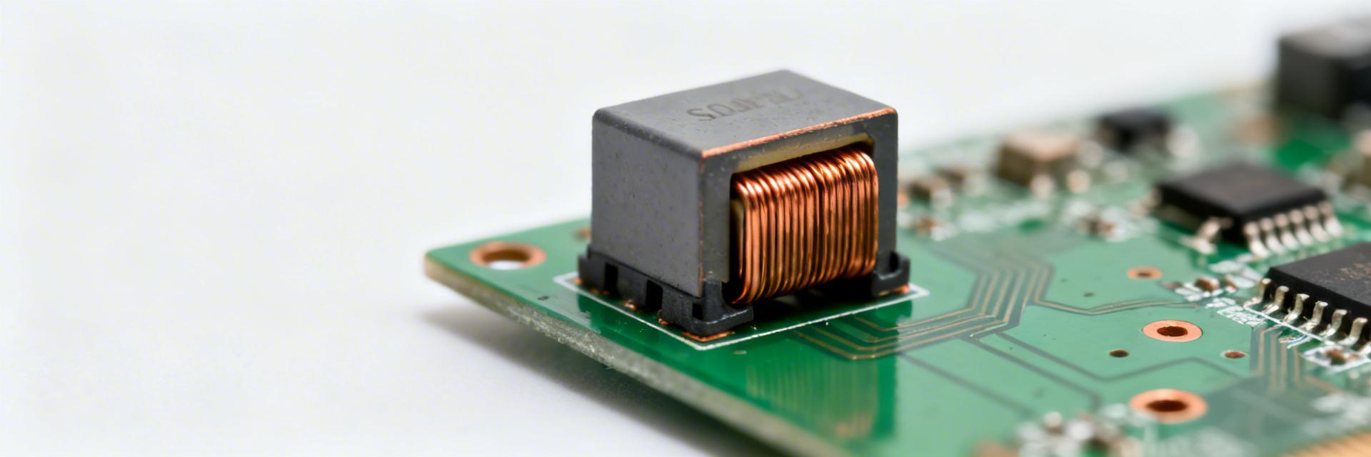
1 — Product overview & key specifications (background)
| Performance Metric | 784778033 (Shielded) | Generic 7x7 Inductor | Design Advantage |
|---|---|---|---|
| DCR Tolerance | ±10% (Typical) | ±20% | Predictable efficiency |
| EMI Shielding | Integrated Ferrite | None / Partial | Lower noise floor |
| Saturation Curve | Soft Saturation | Hard Saturation | Stable under overload |
| Operating Temp | -40 to +125°C | -40 to +105°C | Higher safety margin |
Begin by locating the datasheet table labeled electrical characteristics for 784778033 and confirm the nominal inductance, tolerance band, typical and maximum DCR, Irms and Isat definitions, SRF and the suggested operating temperature range. For quick interpretation: inductance governs low-frequency attenuation and transient energy storage; DCR controls copper loss and steady-state heat; Irms and Isat set continuous and saturation-limited current envelopes; SRF limits effective inductive behaviour at high switching frequencies. Procurement must verify nominal inductance, DCR (typ & max) and current definitions; mounting and soldering details are manufacturing-dependent.
1.1 Mechanical footprint & package
The datasheet package drawing gives board footprint, recommended land pattern and maximum component height for 784778033. Follow the land pattern exactly, verify pad tolerances on incoming parts, and note recommended solder fillet dimensions. For assembly: confirm maximum reflow profile temperature and number of reflow cycles allowed; check component weight and pick-and-place orientation. Actionable note — measure pad centering and overall body size on a sample lot against the drawing to catch any tape-and-reel or molding variations before volume placement.
1.2 Electrical ratings summary
Key electrical entries to extract from the datasheet are nominal inductance and tolerance, DCR (typical and maximum), Irms definition and value, Isat definition and the SRF. Each spec controls a distinct circuit behavior: nominal L affects output ripple and loop dynamics; DCR sets I2R loss; Irms limits continuous current without excessive temperature rise; Isat defines the current where L collapses; SRF indicates the upper frequency where the part stops acting inductively. Flag those values for procurement verification and place them into simulation models.
2 — Electrical performance data & test conditions (data analysis)
Good comparison requires matching test conditions: measurement frequency, temperature, and DC bias. Inductance values are commonly reported at a specified test frequency (for example 100 kHz or 1 MHz) and at 25°C with no DC bias; bias and frequency changes materially alter the effective L. When comparing parts or interpolating performance, always normalize to test frequency and temperature stated in the datasheet.
"When integrating the 784778033 into high-density layouts, I always recommend a Kelvin-sensing layout for the feedback path if you're pushing the Irms limit. Also, watch out for the 'Acoustic Singing' effect—if your PWM frequency is in the audible range, the ferrite structure can vibrate. Always pot the component if operating in noise-sensitive environments."
- Layout Tip: Keep the switch node (Vsw) trace as short as possible to minimize parasitic capacitance.
- Troubleshooting: If L drops unexpectedly, check if your ambient exceeds 85°C, triggering early saturation.
2.1 Inductance vs. frequency, tolerance, and DC-bias behavior
Inductance typically falls with increasing frequency and with DC bias; the datasheet often includes L(f) and L(I) curves. For filter design, the DC-bias curve predicts inductance under load and therefore the low-frequency cutoff and transient energy. Designers should capture the L vs. I curve from the datasheet and, for critical designs, measure L at expected steady DC bias and the converter switching test conditions to validate loop bandwidth and transient overshoot.
2.2 DCR, core losses and efficiency impact
DCR is measured with a four-terminal or Kelvin method to report low-resistance values accurately; datasheets show typical and maximum DCR with test temperature noted. Copper loss estimate: P_cu ≈ I_rms^2 × DCR (use RMS of combined DC and ripple current). Core loss depends on flux swing and frequency; for first-order converter loss estimates, add core loss as a percent of switching loss or use manufacturer core-loss curves. Always propagate DCR and ripple current into thermal simulations to estimate steady-state temperature rise.
3 — Thermal, reliability & environmental limits (data analysis)
Datasheet thermal limits include minimum/maximum operating temperature and sometimes a temperature rise at specified current. Define a derating strategy based on these statements: many inductors require current reductions above a specified temperature to avoid excessive temperature rise or demagnetization. Confirm whether the Irms rating is for 40°C ambient or board-limited cases and whether Isat is specified at a temperature.
Hand-drawn schematic, not an exact engineering circuit diagram.
3.1 Operating temperature, derating, and thermal management
Apply a conservative derating curve: reduce continuous rating progressively with rising ambient or reduced PCB copper. PCB strategies include increasing top-layer copper area, adding thermal vias under and around switch nodes, and separating hot components to improve convection. Aim for continuous operation at least 20–30°C below maximum component temperature to allow transient heating and manufacturing variation.
3.2 Reliability, lifecycle & environmental compliance
Confirm moisture sensitivity level (MSL), permitted reflow cycles, solderability and storage recommendations on the datasheet and request formal statements for RoHS/REACH compliance. For production, request sample test evidence for solderability and MSL and include visual inspection criteria. Ask the vendor for a reliability summary sheet when lifecycle or harsh-environment use is expected.
4 — PCB layout, mounting, and measurement methods (method guide)
Placement and return-path control significantly affect EMI and stray inductance; place the inductor close to the switching node, minimize trace length to the diode or synchronous FET, and provide a short, low-impedance return path. Include the main keyword in layout guidance to highlight component-specific practices and to ensure keyword coverage within the document.
4.1 Recommended PCB footprint & EMI/loop optimization
Do’s: locate the inductor close to the converter output capacitor, keep switching loop area small, use wide traces for current paths, and place input capacitors close to the switching device. Don’ts: avoid routing return currents under the inductor unnecessarily and don’t place sensitive analog traces adjacent to the switching node. Solder paste stencil openings should match the land pattern and favor 0.5–0.7 paste coverage to avoid tombstoning.
4.2 Practical test methods: measuring inductance, DCR, Isat
Use an LCR meter with fixture for low-value inductance, and a Kelvin resistance measurement for DCR. For Isat, apply a controlled DC current and measure L collapse or a defined percent drop point; use temperature control or record temperature when measuring. Avoid warming the part during DCR measurement and calibrate fixtures to remove lead and fixture resistance.
5 — Typical application use-cases & selection guidance (case study)
For synchronous buck converters and point-of-load regulators, prioritize low DCR for efficiency at the expected Irms and sufficient Isat to hold inductance under transient peak current. For LED drivers or high-frequency converters, SRF becomes more important to prevent capacitive behavior. For 784778033, choose operating envelopes based on the datasheet L, DCR and current limits and verify in-system performance with representative switching conditions.
5.1 Use-cases where 784778033 shines
Typical applications include point-of-load supplies and medium-current synchronous buck converters where a compact shielded SMD inductor with documented bias curves is required. Select the inductor when the datasheet shows acceptable DCR at the target current and SRF comfortably above switching frequency to retain inductive behavior.
5.2 Selection checklist vs. competing SMD power inductor specs
Prioritize Isat when transient peak current drives saturation risk; prioritize DCR when steady-state efficiency is critical; prioritize SRF when switching frequency approaches hundreds of kilohertz. Trade-offs: smaller size usually increases DCR; higher Isat often increases size or cost. Use a decision matrix in procurement to weigh these attributes for your design goals.
6 — Procurement, datasheet reading checklist & implementation checklist (action recommendations)
Use a datasheet checklist for purchase decisions and an integration checklist for design sign-off. For 784778033, confirm exact L and tolerance, DCR (typ and max and test temp), Irms and Isat definitions and test conditions, SRF, package drawing, MSL/allowed reflow cycles and recommended reflow profile on vendor documentation.
6.1 Datasheet checklist before purchase
- ✓ Nominal inductance and tolerance — confirm test frequency and temperature.
- ✓ DCR typical and maximum with test temperature stated; request sample DCR measurement.
- ✓ Irms and Isat definitions and measurement methods; request L vs. I curve.
- ✓ Package drawing, maximum height, recommended land pattern and reflow profile; confirm MSL.
6.2 Quick integration & validation checklist for design sign-off
- Pre-silicon: simulate losses using DCR and estimated ripple current; verify thermal margin.
- On-board: measure L and DCR at expected bias and temperature; confirm temperature rise at rated Irms.
- Production: set incoming inspection tests (sample DCR, visual, dimensional) and define go/no-go limits.
Summary
- Critical specs to check: Nominal inductance, DCR (typ & max), Isat/Irms definitions, SRF and maximum operating temperature — all must be confirmed on the datasheet for 784778033 and validated by sample test.
- Top layout and PCB checks: Minimize switching loop area, widen current traces, follow the recommended land pattern and use adequate thermal copper and vias to manage heat.
- Key test / procurement checks: Request L vs. I curves, four-terminal DCR measurements at specified temperature, MSL and reflow limits, and a small-sample electrical verification plan before volume purchase.
- Recommendation: Choose this SMD power inductor when the datasheet shows a balance of low DCR and sufficient Isat for the intended converter envelope and validate with in-system L/DCR/temperature measurements.
Frequently Asked Questions
How should DCR be verified for incoming samples?
Measure DCR with a four-terminal (Kelvin) fixture at the temperature specified on the datasheet; record ambient and part temperature. Use a reference resistor and calibrate the fixture to remove lead resistance. Sample multiple parts to capture lot variation and compare typical and maximum values declared by the manufacturer.
What is the best practical method to determine Isat in the lab?
Apply a controlled DC current ramp while measuring inductance; define Isat as the current where L drops by a specified percent from its zero-bias value (per datasheet definition). Maintain temperature control or log temperature to separate thermal effects from magnetic saturation.
Which layout changes most reduce audible or EMI noise?
Reducing switching loop area and keeping return paths adjacent to the switching node are most effective. Add proper decoupling, route sensitive analog traces away from high dV/dt nodes, and use ground pours with stitched vias to provide low-impedance returns and shielding for the inductor area.


