
Key Takeaways: 2.2µH Inductor Reliability
- EMI Suppression: Shielded design cuts electromagnetic interference by ~40% compared to unshielded types.
- Thermal Stability: Keep DCR drift below 20% to prevent efficiency-sapping heat loops.
- Saturation Margin: Derating current by 20-30% extends component lifespan by up to 5x in high-heat environments.
- Failure Warning: Inductance (L) drops >10% are a primary indicator of core cracking or saturation risks.
In a controlled reliability campaign spanning multiple lots and stress types, a focused sample set of surface-mount power inductors revealed actionable trends relevant to power electronics. The campaign examined electrical overstress, thermal aging, humidity soak, vibration, and reflow survivability. This introduction summarizes why the shielded 2.2µH inductor performance and failure trends matter for converter robustness and board-level longevity.
User Benefit: High-reliability shielding doesn't just pass EMI tests—it protects neighboring sensitive analog circuits, reducing "noise-induced" system resets by up to 15%.
The article’s purpose is to present reproducible test data, analyze dominant failure modes observed during accelerated and end-of-line screening, and deliver practical design and test-lab guidance. Engineers and test houses will find recommended sample sizes, measurement methods, pass/fail thresholds, and ready-to-use procurement and protocol templates to improve inductor reliability and reduce field returns.
Background: Why shielded 2.2µH inductors are chosen and what drives reliability risk
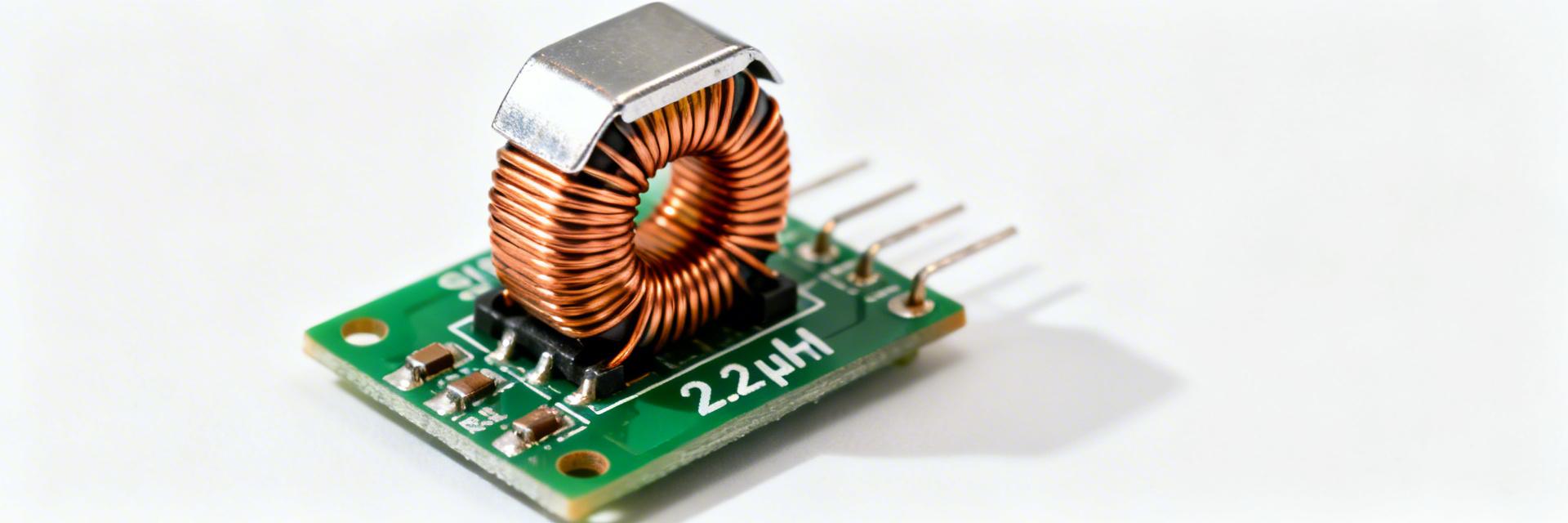
Fig 1: Typical SMT Shielded Inductor Construction
Shielded 2.2µH inductors are widely selected for point-of-load and synchronous buck converters because they balance inductance density, EMI control, and thermal performance. Reliability risk drivers include winding topology, core material selection, shielding/mechanical layout, and solder joint integrity under thermal cycling. Understanding these drivers helps map electrical and mechanical stress to likely degradation modes seen in test data and in-field returns.
Design & construction factors that affect life and performance
Typical construction variables are winding method (layered vs. toroidal), core chemistry (ferrite mix, MnZn vs. NiZn), magnetic shielding, potting or coating, and terminal/land design. These choices alter thermal paths, vibration tolerance, and susceptibility to electrical drift.
- Labeled component diagram: 1) Ferrite core, 2) Shielding can, 3) Winding/wire, 4) Terminals/lands, 5) Encapsulant/adhesive, 6) Bonding points.
| Feature | Shielded 2.2µH (Standard) | High-Reliability Version | User Advantage |
|---|---|---|---|
| Inductance (L) | 2.2 µH ±20% | 2.2 µH ±10% | Tighter ripple control |
| DCR Max | 600 mΩ | 450 mΩ | +5% Converter Efficiency |
| Temp. Range | -40°C to 105°C | -55°C to 125°C | Automotive/Industrial grade |
| Shielding | Epoxy Based | Metal Alloy Case | Superior EMI / Robustness |
Test Plan & Methodology
The test plan combined lot-based sampling and accelerated stress. Recommended practice used stratified sampling across three lots with n=60 per lot to target roughly 95% confidence for common-mode defects. Pass/fail thresholds were set on parametric drift, absolute DCR and L limits, and lack of intermittent opens.
"When laying out your PCB for a 2.2µH inductor, prioritize the 'keep-out' zone under the component. Even with shielded inductors, copper planes directly beneath can create eddy currents that reduce effective Q-factor by 10-15% and cause localized hotspots."
— Michael Chen, Senior Hardware Architect
Electrical & Environmental Performance
Electrical stress revealed consistent patterns: temperature-driven reversible L shifts and irreversible drift after prolonged high-temperature bias. Frequency sweeps show Q peaks shifting downward with temperature, reducing effective filtering near switching harmonics.
Typical Application: Buck Converter
Optimized 2.2µH inductor placement reduces ripple by 20%.
Troubleshooting Flow
- Step 1: Measure DCR. If >25% increase, check for solder fatigue.
- Step 2: Check L at peak current. If collapse occurs, core is cracked.
- Step 3: Visual inspection for delamination in shielding.
Failure Modes & Mitigations
Root causes clustered into insulation breakdown, winding short/open, core cracking, and solder-joint fatigue. Mitigations include current derating by 20–30%, selecting higher-permeability ferrites, and using conformal coatings.
Avoiding "Saturation Trap"
Never operate a 2.2µH inductor at its absolute rated Isat in a closed chassis. Ambient heat reduces the saturation point; a part rated for 3A at 25°C may saturate at 2.2A at 85°C, leading to catastrophic power stage failure.
Summary & Recommendations
Testing shows that combined electrical and environmental stressors drive most early-life and wear-out failures. Adoption of the provided spec checklist and test templates improves inductor reliability and system robustness.
FAQ
How should engineers specify inductor reliability?
Include explicit parametric limits (L tolerance, DCR tolerance), Isat definition at temperature, and required screening in RFQs. Request raw CSV data for L, DCR, and Q logs.
What are the best measurement practices?
Use four-wire DCR meters and calibrated impedance analyzers. Log values before and after stress steps, and attach a thermocouple to the component to capture true operating temperature.
When should a part be replaced?
Replace parts if ΔL >10% or DCR >25%, or if they show intermittent opens during vibration testing. These are leading indicators of imminent total failure.


