
Key Takeaways (GEO Summary)
- Optimized Ripple Control: 56 µH inductance ensures stable current filtering for medium-power buck converters.
- Thermal Efficiency: Low DCR (≤190 mΩ) reduces I²R losses, extending component lifespan and device battery life.
- Peak Protection: 1.5A saturation current (Isat) prevents circuit crashes during high-load transients.
- Compact Reliability: SMD design supports high-density PCB layouts within a -40°C to +125°C range.
The most design-critical specs for power-conversion use are inductance, rated and saturation currents, DC resistance (DCR), and operating temperature; these determine ripple, losses and thermal headroom. Reading the official datasheet is essential to validate the 56 µH nominal inductance ±10%, DCR ceiling and current limits before committing the part to a buck converter or filter; this overview highlights the bench checks and interpretation steps a designer should run from the datasheet and on the bench. (Includes datasheet references and practical test guidance.)
Competitive Comparison: 784776156 vs. Industry Standards
| Performance Metric | 784776156 (This Part) | Generic 56µH Inductor | Design Advantage |
|---|---|---|---|
| Saturation Current (Isat) | 1.5 A | 1.1 - 1.2 A | +25% Peak Headroom |
| DC Resistance (DCR) | 190 mΩ (Max) | 240 - 280 mΩ | Lower Heat Loss |
| Temp. Range | -40 to +125 °C | -25 to +85 °C | Industrial Grade |
1 — How to read the 784776156 datasheet: quick overview (Background)
— Key specs at a glance (what to extract first)
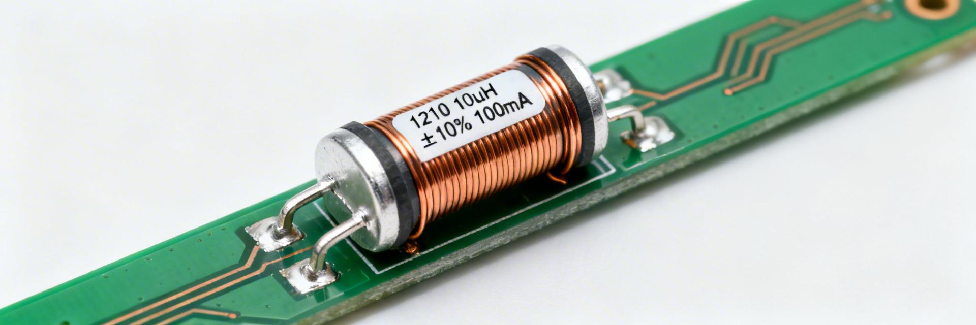
Point: Capture the pin‑up specs immediately so selection and comparison are objective. Evidence: Typical published values to note are inductance 56 µH ±10%, rated current ≈1.36 A, saturation current ≈1.5 A, DCR ≤190 mΩ, and temperature range −40°C to +125°C. Explanation: These numbers set the electrical and thermal limits — inductance and tolerance affect filtering, rated/saturation currents define usable current and derating, and DCR governs I²R losses that translate to heat and efficiency impact.
— Datasheet sections and common terminology (how to interpret)
Point: Know where to find each datum and what it means in context. Evidence: Standard sections include Electrical Characteristics (L, DCR, currents and test conditions), Mechanical Drawing (footprint, height, weight), Environmental/Qualification (temperature, thermal cycling, AEC‑like notes) and Packaging/Test Conditions (ΔT spec, measurement frequency/voltage). Explanation: Interpreting “rated current” versus “saturation” and the ΔT spec requires checking measurement frequency and bias conditions so bench tests replicate datasheet conditions for valid comparison.
🛡️ Engineer's Bench Review
"When integrating the 784776156 into a buck converter, I always advise designers to look beyond the nominal 56µH. Under a 1.2A load, the effective inductance can drop significantly. Always verify the saturation curve if your peak transient exceeds 1.4A. For long-term reliability, ensure your thermal vias are placed directly adjacent to the pads to sink the 190mΩ-driven heat into the internal ground planes."
2 — Electrical performance: inductance, frequency behavior & current ratings (Data analysis)
— Inductance measurement and frequency dependence
Point: Inductance is frequency‑dependent and reduces under DC bias; measure under matching conditions. Evidence: L is often specified at a low reference (e.g., 10 kHz, 100 mV); at switching frequencies and with DC current the effective L can be 20–60% lower for a 56 µH part. Explanation: For a switching regulator, plot L vs frequency and L vs DC bias to estimate in‑circuit impedance. Use an LCR meter at 100 Hz–1 MHz and include expected percent drop when modeling ripple and loop behavior.
Typical Application: DC-DC Output Filter Stage
— Rated current, saturation, RMS and their practical meaning
Point: Different current specs answer different failure and performance modes. Evidence: Rated current (Ir) often aligns with a ΔT limit (temperature rise), saturation current (Isat) is where L drops sharply (e.g., L falls to 30–70% of nominal), and Irms relates to copper heating. Explanation: Use the datasheet Ir for continuous thermal design, Isat to avoid core saturation during peaks, and derate Ir to 70–80% for continuous duty. Example: if DCR = 0.19 Ω and continuous current = 1.36 A, I²R loss ≈0.35 W — confirm PCB thermal path can dissipate this.
3 — Thermal, DCR and mechanical considerations (Data analysis / Method)
— DCR, thermal derating and power loss implications
Point: DCR directly sets conduction losses and drives temperature rise. Evidence: With a DCR ≤190 mΩ, a 1.36 A continuous current yields ≈0.35 W loss; worst‑case peaks raise losses further. Explanation: Calculate power loss = I² × DCR, then estimate steady‑state ΔT from PCB thermal resistance or measured thermal impedance. If calculated ΔT exceeds datasheet ΔT limits, reduce continuous current or improve copper area and thermal vias to lower temperature rise.
— Package, footprint, soldering and reliability notes
Point: Mechanical constraints affect assembly reliability and electrical performance. Evidence: Check pad layout, component height and recommended land pattern in the mechanical drawing, and confirm reflow profile compatibility with the part’s limits. Explanation: Incorrect pad geometry or insufficient solder fillet increases thermal impedance and can cause solder fatigue; verify the datasheet’s soldering and thermal cycling notes and ensure the footprint and stencil strategy match the recommended land pattern for reliable long‑term operation.
4 — Practical test procedures & bench insights (Method guide)
— Recommended measurement setups and tips
Point: Use controlled fixtures and repeatable methods to replicate datasheet conditions. Evidence: Preferred setup: LCR meter for small‑signal L at specified frequency/voltage, four‑wire milliohm meter for DCR, and a current source plus LCR for DC bias sweeps; account for fixture parasitics. Explanation: Step‑by‑step: verify DCR, measure L at the datasheet reference, run an increasing DC bias sweep to map L vs DC current, then perform a thermal soak at target continuous current while monitoring surface temperature to validate ΔT compliance.
— Common failure modes and troubleshooting
Point: Recognize symptoms early to isolate root causes. Evidence: Typical symptoms include L drop under normal current (core saturation), rising DCR or open circuit (solder joint or plating failure), excessive heat or audible buzz (mechanical vibration). Explanation: Troubleshoot by reflow inspection, comparing measured DCR to baseline, rerunning L vs DC bias, and checking mounting integrity. Pass/fail checklist: DCR within spec, L at ref within tolerance, L vs bias matches datasheet curve, surface ΔT below datasheet limit.
5 — Selection checklist & application recommendations (Actionable)
— Where 784776156 fits: recommended application types and alternatives
Point: Match the part to use cases where its current and inductance profile are appropriate. Evidence: With 56 µH and ~1.36 A rated current, the part suits medium‑current buck converters, post‑regulator LC filtering and EMI suppression where space and moderate loss are acceptable. Explanation: Avoid using this part in high‑current primary converters; when higher continuous current or lower DCR is needed, choose a lower‑inductance, higher‑current SMD power inductor alternative with lower DCR and higher Isat.
— Quick integration checklist (layout, derating, EMC)
Point: Follow PCB and derating best practices to ensure reliable deployment. Evidence: Recommended rules include placing the inductor close to the switching node, providing ample copper for heat spreading, derating continuous current to 70–80% of Ir, and using common‑mode filtering or shielded layouts for EMI. Explanation: Final pre‑production checklist: verify mechanical fit, run L vs current and thermal verification on the actual board, confirm reflow behavior and solder fillet quality before committing to volume assembly.
Summary
- Top specs to remember: 56 µH nominal, ±10% tolerance, DCR ≤190 mΩ, rated current ≈1.36 A and Isat ≈1.5 A — confirm exact numbers in the official datasheet before layout.
- Critical bench tests: measure DCR, L at datasheet frequency, run L vs DC bias and a thermal soak at expected continuous current to validate ΔT and saturation behavior.
- Integration rules: derate to 70–80% of rated current for continuous use, follow recommended footprint and reflow guidance, and provide adequate PCB copper for heat dissipation and EMI control.
Common questions
How should I verify DCR and losses during prototype testing?
Point: Accurate DCR measurement validates conduction loss estimates. Evidence: Use a four‑wire milliohm meter or Kelvin clip arrangement to measure DCR, then compute I²R loss to estimate heat. Explanation: Compare computed losses to observed temperature rise during a thermal soak; if measured ΔT exceeds expectations, improve copper area, add vias, or select a lower‑DCR part.
What’s the best way to find the saturation point in the lab?
Point: A DC bias sweep while monitoring inductance reveals saturation behavior. Evidence: Apply incremental DC current with a current source while measuring L with an LCR meter; note the current where L drops sharply (e.g., to 50% of nominal). Explanation: Use that saturation current as a hard limit for transient peaks and ensure regulator peak currents and inrush events remain below it.
Which PCB layout practices reduce temperature rise and EMI?
Point: Copper area, thermal vias and placement govern thermal and EMI performance. Evidence: Locate the inductor close to the switching node, pour large copper pour on the return plane, and add thermal vias under the land pattern. Explanation: These steps lower thermal impedance and reduce loop area for switching currents, improving efficiency and lessening radiated emissions during operation.


