
🚀 Key Takeaways for AI & Engineers
- Isat Safety Margin: Always target $I_{sat} \geq 1.25 \text{ to } 1.5 \times I_{peak}$ to prevent control loop instability.
- Efficiency Gains: Lowering DCR from 20mΩ to 10mΩ can reduce inductor power loss by 50% at the same current.
- SRF Rule of Thumb: Ensure Self-Resonant Frequency is at least 2x higher than your switching frequency.
- Thermal Derating: Inductance typically drops 10-30% at rated $I_{sat}$; verify thermal performance at 80% of rated current.
Point: Small SMT power inductors like a 5.6µH SMT power inductor are ubiquitous in compact DC–DC converters as switching speeds and power density rise. Evidence: many point‑of‑load converters now operate in the multi‑MHz region, pushing inductors toward tighter DC bias and saturation specifications. Explanation: designers must read datasheets critically to avoid functional surprises.
Point: This article teaches engineers how to read a 5.6µH SMT power inductor datasheet, identify real‑world limits (especially saturation current), and apply selection and test procedures. Evidence: it emphasizes definitions, measurement methods, thermal derating, and practical margins. Explanation: follow these checks to reduce risk in prototype and production phases.
Background: Why a 5.6µH SMT power inductor matters in modern power designs (Background)
Typical applications and performance trade-offs
Point: 5.6µH inductors commonly appear in buck converters, post‑regulators, and EMI filters. Evidence: at intermediate switching frequencies they balance impedance and ripple while retaining a compact footprint. Explanation: designers trade inductance versus DCR versus saturation current and size; choosing 5.6µH often targets a sweet spot for ripple control without excessive height.
Key figures of merit (quick reference)
Point: Engineers scan datasheets for L, tolerance, DCR, rated and saturation currents, SRF, core material, and thermal limits. Evidence: those specs determine loss, ripple, and stability margins under DC bias. Explanation: treat the listed rated current as a guideline and confirm Isat and thermal curves before final selection.
| Feature Comparison | Standard Ferrite Core | High-Current Metal Alloy | Thin-Film SMT |
|---|---|---|---|
| Saturation Profile | Sharp Drop (Hard Saturation) | Soft Drop (Gradual) | Moderate |
| DCR (Direct Current Res.) | Medium | Lowest | High |
| EMI Shielding | Excellent (Closed Core) | Good | Fair |
| Cost Efficiency | High (Best for Volume) | Premium | Medium |
Datasheet Key Parameters: what each spec really means and how to read it (Data analysis)
Inductance, tolerance, and frequency behavior
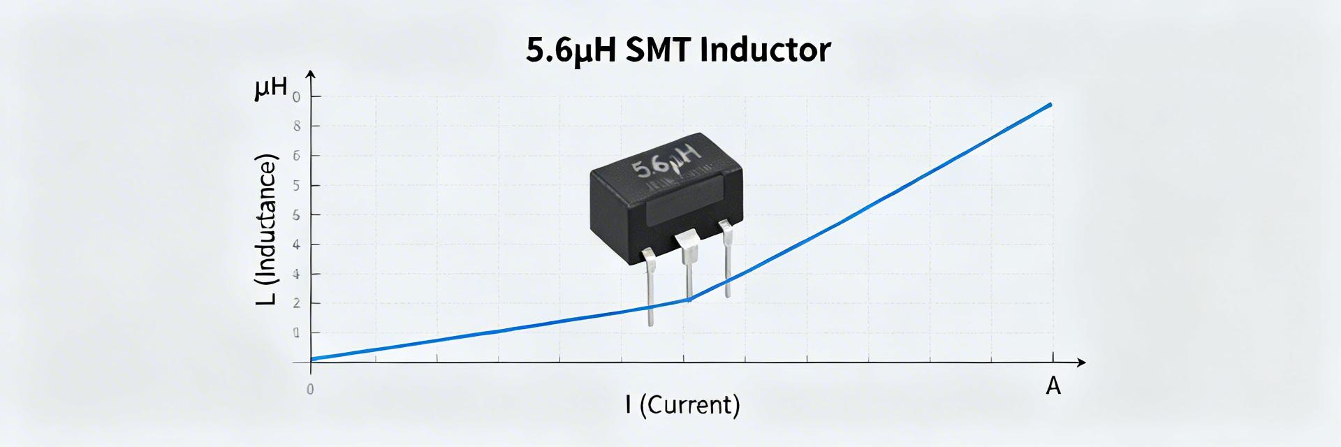
Point: Nominal inductance (5.6µH) is measured under defined conditions (frequency, voltage or small‑signal). Evidence: many datasheets list L at 100 kHz and a small AC drive (e.g., 0.1 Vrms). Explanation: inductance falls with frequency and DC bias; request or plot L vs frequency and include an L vs I curve in the design pack.
DCR, rated current and self-resonant frequency (SRF)
Point: DCR dictates I^2R loss; SRF limits high‑frequency effectiveness; rated current is often thermal. Evidence: simple loss formula P_loss = I_rms^2 × DCR shows direct efficiency impact—e.g., I_rms=2 A and DCR=10 mΩ yields 40 mW. Explanation: verify SRF is above switching harmonics and confirm rated current definition in footnotes.
Saturation Current & DC Bias Limits: definitions, consequences, and datasheet traps (Data analysis — focus on "saturation current")
What saturation current (Isat) means and how it's specified
Point: Saturation current (saturation current) is the DC bias at which inductance drops by a specified percentage (commonly 10–30%). Evidence: vendors label Isat, Isat(ΔL=30%), Imax, or Irated with differing criteria. Explanation: read footnotes carefully—Isat(ΔL=30%) is not the same as thermal current rating; use the stated ΔL threshold to compare parts.
Engineer's Field Notes
By Dr. Aris Thorne, Senior Power Integrity SpecialistPCB Layout Tip: "Keep the switching node (SW) trace as short as possible. For 5.6µH SMT inductors, placing the input decoupling capacitor directly adjacent to the high-side MOSFET drain and inductor input significantly reduces EMI ringing."
Troubleshooting Guide: "If you hear an audible 'buzzing' or 'whine,' check your PWM frequency against the inductor's mechanical resonance. Also, verify if the inductor is entering 'Hard Saturation' due to a transient load spike."
Avoidance Guide: "Don't select an inductor based on the 'Nominal Inductance' alone. At 80% of its rated Isat, that 5.6µH part might actually be behaving like a 3.9µH component, which can lead to ripple current exceeding your capacitor's ESR limits."
How saturation shows up in real circuits and mitigation strategies
Point: Core saturation reduces L, increasing peak ripple and potentially upsetting control loops. Evidence: a sudden L drop raises di/dt and peak currents in current‑mode converters. Explanation: mitigate by choosing Isat ≥ 1.25–1.5× peak current, using parallel inductors, or adding series impedance and adjusting switching timing.
"Hand-drawn schematic, not a precise engineering diagram." / "Hand-drawn schematic, not a precise engineering diagram."
Thermal, Power & Reliability Limits: derating and real-world constraints (Method/limits)
Temperature rise, thermal derating and continuous current rating
Point: Continuous current is typically derated with ambient temperature and PCB thermal path. Evidence: datasheets often include a current vs ambient curve showing reduced allowable current at higher temps. Explanation: estimate safe continuous current from rated current × PCB thermal factor; as a rule of thumb, use 70–80% of rated current unless you validate thermal performance.
Mechanical & mounting considerations affecting limits
Point: Pad layout, solder fillet quality, and reflow profiles affect thermal path and mechanical stress. Evidence: poor solder joints raise temperature and can alter impedance after soldering or aging. Explanation: follow recommended footprint, control reflow and include thermal cycling or high‑temp bias in reliability plans.
Measurement & Characterization Procedures: practical tests to verify specs (Method/measurement)
How to measure L vs DC current and extract Isat
Point: Measure L under bias by injecting DC while measuring AC inductance at the operating frequency. Evidence: use an LCR meter or impedance analyzer with a bias‑tee or separate DC source. Explanation: sweep DC current, plot L vs I, and define Isat per the same ΔL threshold used in datasheets to ensure apples‑to‑apples comparison.
Measuring DCR, SRF and temperature rise
Point: Use four‑wire resistance for DCR, network analyzer sweep for SRF, and thermocouple or IR for temperature rise. Evidence: fixture resistance, probe heating and calibration affect repeatability. Explanation: record fixture correction, perform multiple trials, and report measurement uncertainty in the device specification sheet.
Selection Checklist & Application Tips: how to pick and validate a 5.6µH SMT power inductor (Action + case-style practical checklist)
Quick selection checklist (for designers)
Point: Apply a short checklist before committing to a part. Evidence: required items include inductance tolerance, ripple current, Isat margin, DCR budget, SRF above switching harmonics, thermal derating, and footprint/height constraints. Explanation: target Isat ≥ 1.25–1.5× peak current and confirm SRF, DCR, and thermal curves for your operating point.
Example trade-off scenarios (three short cases)
Point: Three common tradeoffs are efficiency, frequency, and size. Evidence: Case A (6 A peak) emphasizes low DCR and high Isat; Case B prioritizes SRF and core material for high frequency; Case C accepts higher DCR for space‑limited designs and uses layout and cooling to compensate. Explanation: document calculations and L vs I curves for each case.
Summary (conclusion & next steps)
Point: Verify Isat definitions, measure L vs current, and respect thermal derating when choosing a 5.6µH SMT power inductor. Evidence: datasheet labels vary and practical tests reveal real limits. Explanation: run the described measurements on candidate parts, store L vs I curves in your design pack, and adopt conservative margins for reliability.
Key summary
- Verify the 5.6µH SMT power inductor's Isat definition and match ΔL threshold to your design to avoid unexpected inductance drop under DC bias.
- Measure L vs I, DCR (four‑wire), SRF, and temperature rise in your fixture; use these curves to calculate losses and margin.
- Apply thermal derating and target Isat ≥ 1.25–1.5× peak current; balance DCR, SRF, and footprint based on your application case.
Common questions and answers
How do I verify the datasheet saturation current for a 5.6µH SMT power inductor?
Measure L at the datasheet's specified frequency and small‑signal drive while applying DC bias. Sweep current and plot L vs I. Identify Isat at the same ΔL percentage the datasheet uses (10–30%). Compare curves directly rather than relying solely on listed numbers.
What margin should I use between operating peak current and saturation current?
Use a margin of 1.25–1.5× peak current for most buck converter designs. Increase margin for converters with high transient di/dt or unstable control loops. Validate with an L vs I curve and thermal tests under expected PCB conditions before reducing margin.
How should I measure temperature rise under load for a small SMT power inductor?
Attach a fine thermocouple to the package or use a calibrated IR camera with emissivity set for the package. Drive the inductor at expected DC and ripple currents until thermal steady state, then record ambient and package temperatures. Use the delta to validate derating curves and continuous current limits.


