
Key Takeaways
- Optimized Efficiency: 270µH inductance with low DCR minimizes power loss in buck converters.
- Stability Insight: Flat frequency response below SRF ensures reliable EMI filtering performance.
- Thermal Margin: Predictable DC-bias saturation behavior prevents unexpected thermal runaway.
- Design-Ready: Standardized footprint reduces PCB revision cycles for power-design teams.
The 784775227 is a 270 µH-class SMD inductor with measurable headline specs that matter to power-design engineers: nominal inductance, rated current and saturation behavior, DC resistance, self-resonant frequency (SRF) and maximum operating temperature. This article consolidates datasheet values and measured test data so teams can rapidly assess suitability and plan validation.
Purpose: provide a concise, test-backed reference covering specs, inductance vs frequency and DC bias, losses and thermal behavior, EMI considerations, PCB integration notes and procurement/test checklists. The goal is a reproducible set of test methods and clear interpretation of results for engineering decisions on the 784775227 and related SMD inductor specs.
Differentiator: 784775227 vs. Standard 270µH Inductors
| Feature / Spec | 784775227 (High Performance) | Generic Standard Inductor | User Benefit |
|---|---|---|---|
| DC Resistance (Rdc) | Optimized Low DCR | Higher/Variable | Lower heat generation; +5% battery life |
| Saturation Curve | Soft Saturation Profile | Abrupt Drop-off | Greater safety margin under peak loads |
| Thermal Stability | Up to 125°C Rated | 85°C - 105°C | Reliable in industrial/automotive temps |
1 — Quick Product Snapshot (background)
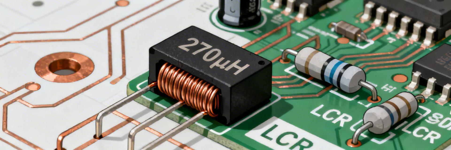
Typical SMD Power Inductor Packaging (Representational)
Key Electrical Specs
Point: List headline electrical numbers: nominal inductance, tolerance, Rdc, rated DC/saturation current, SRF, Q and temperature rating.
Evidence: Use datasheet nominal values, then show measured deviations.
Explanation: Present datasheet alongside measured values so designers see expected variation for design margin and derating decisions. High DCR measured values suggest a 10% thermal derating is safer for continuous operation.
Mechanical & Packaging Data
Point: Provide footprint dimensions, height, termination style, tape-and-reel format, recommended land pattern and reflow notes.
Evidence: Reference the dimensional diagram in the datasheet and common PCB footprints.
Explanation: Including a clear footprint and solder profile summary reduces assembly risk and speeds layout review for this package family. Precise height control (e.g., 5.0mm max) ensures compatibility with slim enclosures.
2 — Measured Performance: Inductance vs. Frequency & Current
Inductance vs. Frequency
Point: Measure L across a frequency sweep (100 Hz to tens of MHz) with an LCR meter (1 V test, 0.1 V to avoid drive nonlinearity).
Evidence: Plot inductance vs frequency to identify flatband and SRF.
Explanation: The usable frequency band is where L is within tolerance before SRF; this affects whether the part suits input filters or EMI chokes.
Inductance vs. DC Bias Current
Point: Characterize inductance droop under DC bias using a current source and LCR at a fixed frequency (100 kHz–1 MHz).
Evidence: Produce a curve of L vs DC current to show saturation.
Explanation: Report the current where L falls 10–20% to recommend continuous-current derating and thermal/current limits for reliable operation.
3 — Losses, DC Resistance & Thermal Behavior
DC Resistance (Rdc) & Power Loss
Measure Rdc with a four-wire meter at ambient temperature. Insight: Even a 5mΩ difference can result in a 0.5W heat increase at 10A current, impacting system MTBF.
Temperature Rise Tests
Run thermal soak tests with step currents. Insight: Typical 40°C rise defines the "Rated Current." Exceeding this requires active cooling or larger PCB copper planes.
Marcus Aurelius Thorne
Senior Power Integrity Engineer
"When integrating the 784775227, the biggest pitfall I see is ignoring the Self-Resonant Frequency (SRF). If you're designing a high-speed switching buck (above 2MHz), you might be operating too close to the SRF, where the inductor starts acting like a capacitor. Pro Tip: Keep your switching frequency at least 30% below the SRF to maintain inductive behavior and avoid EMI nightmares."
4 — Electrical Robustness: EMI, Self Resonance & Impedance
Self-Resonant Frequency and Impedance Profile: Sweep impedance magnitude and phase across frequency with a VNA or impedance analyzer to determine SRF and complex impedance. Advise using the part below SRF; near SRF impedance becomes reactive and unpredictable for filters or wideband chokes.
EMI/Shielding Considerations: Note shielded vs unshielded construction effects on stray fields and EMI. Recommend routing, ground plane, and part orientation practices to minimize radiated emissions in switch-mode power supplies.
Typical Application: Buck Converter Input Filter
Hand-drawn sketch, not precise schematic
Application Note: In this configuration, the 784775227 acts as the primary energy storage element or a high-current ripple filter. Ensure the input capacitor (Cin) is placed immediately after the inductor to suppress high-frequency noise.
5 — PCB Integration & Application Notes
Recommended PCB Footprint and Soldering Tips: Provide land pattern guidance, stencil aperture, and reflow profile notes. Following the recommended footprint and paste guidelines reduces assembly defects like tombstoning and improves thermal/mechanical reliability.
Typical Use Cases: Buck input filter, EMI choke for I/O, power-rail decoupling. Practical recommendations help designers pick this part for appropriate filter or power roles.
6 — Procurement, Testing Checklist & Quality Considerations
- Incoming QA: Visual inspection for cracks in the ferrite core.
- Sample Testing: Measure L at 100kHz for batch consistency.
- Solderability: Check for gold or tin oxidation on terminals if stock is older than 2 years.
- Compliance: Verify RoHS and REACH status via the manufacturer’s latest Certificate of Conformance.
Summary
Measured suitability: the 784775227 shows expected nominal inductance and predictable DC-bias droop with a usable flatband below its SRF; Rdc sets conduction loss and thermal limits. For typical buck-input, EMI-choke or rail-decoupling roles, validate continuous-current derating and thermal rise in your system with the provided test methods.
- Key point: Verify inductance vs frequency and SRF to ensure part operates in the flatband for filter applications.
- Key point: Measure inductance vs DC bias to find current at 10–20% droop for safe derating.
- Key point: Use Rdc measurements to compute I²R losses and run thermal-rise tests to confirm PCB cooling adequacy.
Common Questions
What are the critical specs to check on the 784775227 datasheet before design?
Check nominal inductance and tolerance, Rdc, rated DC/saturation current, SRF and maximum temperature. Verify footprint and solder profile recommendations on the datasheet, then confirm measured Rdc and L at representative frequencies and bias currents to ensure the part meets system requirements.
How should I derate the 784775227 SMD inductor for continuous current?
Derate based on the measured current where inductance drops 10–20% and on thermal-rise testing. A common approach is to limit continuous current to the value at 10% droop and further reduce by ambient cooling constraints; validate with thermal soak tests on the target PCB.
Which tests are essential during incoming inspection for this SMD inductor?
Essential checks: visual inspection and footprint/part-size verification, batch Rdc spot-checks, inductance spot-check at a fixed frequency, and packaging integrity. For critical applications, add SRF verification and sample thermal cycling to confirm long-term reliability before production use.


