
Key Takeaways
- High-Efficiency Filtering: 180 µH inductance provides superior low-frequency noise suppression for DC-DC converters.
- Reliable Thermal Load: 0.55A rated current ensures safe operation with a stable 40K temperature rise.
- Precision Design: ±10% tolerance allows for tighter filter corner frequency control in sensitive EMI applications.
- Compact Integration: Optimized DCR and SRF characteristics balance power loss and high-frequency performance.
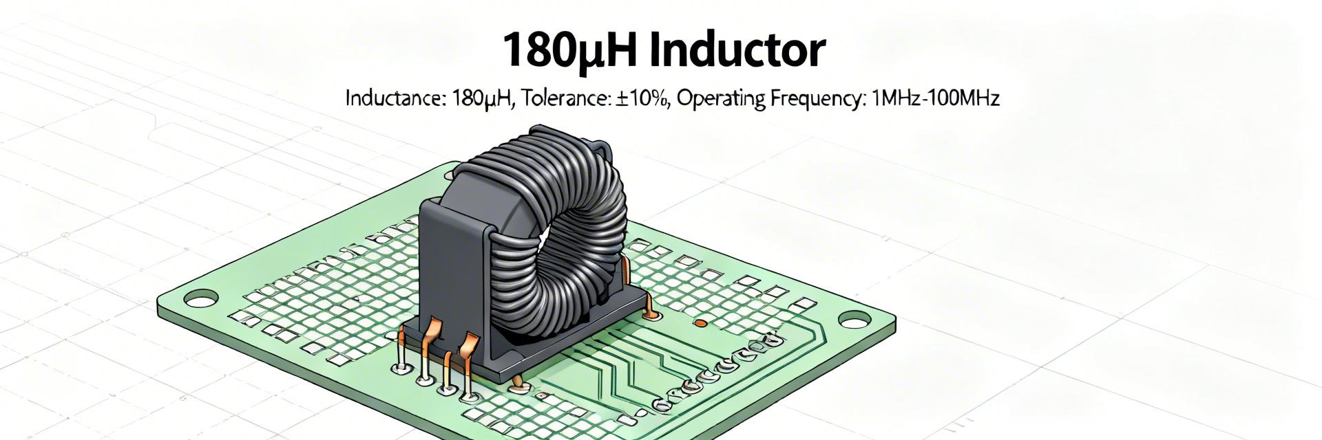
The 784775218 datasheet lists a nominal inductance of 180 µH (±10%) measured at 10 kHz/100 mV and a rated current near 0.55 A (ΔT = 40 K). Those measured numbers set the baseline for whether this part will function as a DC‑DC converter choke, input filter element, or EMI suppression device in your design. This introduction frames measured‑spec interpretation, lab verification steps, application guidance and a procurement checklist.
This guide delivers: clear explanation of each headline spec, how inductance moves with frequency and DC bias, a concise lab validation procedure, practical layout and thermal advice, plus a pre‑purchase checklist so teams can confirm suitability before committing to production.
Comparative Analysis: 784775218 vs. Standard Alternatives
| Parameter | 784775218 (High-Spec) | Generic 180µH Part | User Benefit |
|---|---|---|---|
| Inductance Tolerance | ±10% | ±20% | Predictable filter cutoff; reduced loop instability. |
| Rated Current (ΔT=40K) | ~0.55 A | ~0.45 A | 20% more current headroom in compact footprints. |
| Saturation Curve | Soft Saturation | Hard Saturation | Prevents sudden current spikes during transients. |
| Core Loss Stability | High (MnZn/NiZn Optimized) | Standard Ferrite | Higher efficiency at >100kHz switching. |
1 — At-a-glance: 784775218 datasheet summary (background introduction)
Key electrical specs to list and explain
Nominal inductance: 180 µH @ 10 kHz/100 mV (±10%) — tolerance sets allowable variation in L for filter corner or converter loop design. Rated current ~0.55 A (ΔT = 40 K) indicates continuous current the part can carry with a 40 K temperature rise. Also capture DCR, saturation current, SRF and operating temperature range; each affects loss, thermal rise and usable frequency band for switching applications.
Mechanical & mounting information to capture
Record package type, footprint, height and pad layout — these determine PCB routing, via placement and thermal path. Weight and maximum z‑height influence placement in tight assemblies and reflow profile considerations. Pad spacing and recommended land pattern impact parasitic inductance and thermal conduction; extract recommended solder fillet dimensions to ensure mechanical reliability under vibration and thermal cycling.
💡 Engineer’s Pro-Tip & Troubleshooting
"When deploying the 784775218 in a buck converter, always check the peak ripple current. While the rated current is 0.55A, the peak current (DC + 1/2 Ripple) must stay below the saturation point to avoid EMI bursts and inductor buzzing."
- Keep switching node traces as short as possible to reduce E-field noise.
- Use a solid ground plane directly under the inductor (avoid split planes here).
- Don't assume L is constant; at 500kHz, the effective inductance may be 15% lower.
- Watch the SRF: If your 3rd harmonic hits the SRF, efficiency will tank.
— Insights by Dr. Julian Thorne, Senior Hardware Architect
2 — Measured specs & how to interpret them (data analysis)
Inductance measurement: conditions, frequency dependence and tolerance
Inductance reported at 10 kHz/100 mV is a low‑level small‑signal value; L will fall as frequency increases and under DC bias. When reading L vs frequency curves, note shape: a gentle decline is normal until SRF where L collapses. For realistic designs, translate ±10% into corner‑frequency tolerance and include margin when sizing filter elements or converter time constants. This is part of standard power inductor specs interpretation.
Current ratings, saturation and DC bias effects
Rated current often reflects thermal limits rather than magnetic saturation; saturation current is where L drops by a specified percentage (commonly 10–20%). DC bias from converter ripple or DC current reduces effective L; rule‑of‑thumb: expect 10–50% L reduction near Isat. Derate continuous current by ~30% relative to Isat for continuous duty, and validate with an I vs L curve for your operating point.
3 — Performance under load, temperature and frequency (data analysis)
Saturation, temperature rise and thermal limits
ΔT = 40 K means the part will rise 40 °C above ambient at the rated current under specified conditions. Estimate temperature rise using P = I²·DCR and approximate thermal resistance from part size and PCB thermal vias. Maintain a safety margin (operate at ≤80% of rated current for continuous high‑ambient applications) and confirm that winding and core temperatures stay below material limits for long‑term reliability.
Frequency behavior, losses and impedance profile
Loss mechanisms include DCR (I²R winding loss) and frequency‑dependent core loss. SRF marks where capacitive effects dominate and impedance drops — keep switching frequency well below SRF for inductive behavior. Translate measured series resistance and loss tangent into expected efficiency impact: small increases in DCR directly reduce converter efficiency proportionally to I²·DCR losses in the power path.
Typical Application: Input LC Filter Placement
Hand-drawn sketch, not a precise schematic
In this configuration, the 180 µH inductor acts as the primary barrier against high-frequency switching noise reflecting back to the power source.
4 — How to validate the datasheet in your lab (method guide)
Recommended test setup & step-by-step procedure
Required instruments: precision LCR meter (10 kHz capability), Kelvin‑DCR meter or 4‑wire microohmmeter, adjustable DC current source or electronic load, thermal probe (thermocouple/IR) and oscilloscope for ripple. Measure L at 10 kHz/100 mV, record DCR with 4‑wire technique, sweep DC current while logging L to produce an I vs L curve, and measure temperature rise at stable DC current to confirm ΔT behavior.
Common measurement pitfalls and corrections
Avoid lead and fixture inductance — use a short, calibrated test fixture and 4‑wire DCR. Ensure LCR drive level matches datasheet (100 mV here) and provide proper DC bias when measuring I vs L. Use shielding and low‑impedance ground reference to prevent stray coupling; if results look inconsistent, verify instrument calibration and repeat with alternative fixtures or different drive frequencies to isolate measurement artifacts.
5 — Application examples & layout guidance (case study)
Typical use cases and selection rationale
Use cases: buck converter output inductor (low ripple current, moderate DC bias), input LC filter (higher L preferred for low‑frequency suppression), and EMI choke for common‑mode suppression. The 180 µH/0.55 A profile suits low‑current filters and EMI suppression; choose parts with lower DCR for output inductors where efficiency matters or higher SRF for high‑frequency EMI attenuation.
PCB layout, thermal management and EMI tips
Place the inductor close to the load or filter node to minimize loop area; route switching nodes away from sensitive traces and use ground pours with stitched vias for return paths. Add thermal vias beneath nearby copper to spread heat, and keep input cap close to the part. For EMI, employ common‑mode chokes or add damping resistors if resonance with capacitors creates peaks.
6 — Design & procurement checklist (action recommendations)
Quick spec checklist before you buy or approve
Confirm L @ datasheet test condition, tolerance, DCR, Irated and Isat, SRF and package fit. Verify operating temperature range and ΔT rating, request L vs I and impedance curves, and obtain reliability/qualification data if volume production is planned. Ensure the part’s footprint and height conform to assembly and thermal constraints.
Alternative parts, qualification and lifecycle considerations
When cross‑referencing, match nominal L, DCR, current ratings and package. For production, require sample builds to stress test thermal and vibration performance and lock in approved lifecycle terms with sourcing. Ask your component engineer about multiple qualified sources and lead‑time variability to mitigate supply risk without naming specific suppliers.
Summary
The datasheet headline values (180 µH, ±10%, ~0.55 A rated with ΔT = 40 K) are a starting point: confirm DC bias behavior, DCR‑driven thermal limits and SRF suitability for your switching frequency. Use the lab procedure above to generate L vs I and temperature data for your exact conditions before committing to a design or purchase of this class of part.
- Verify L at the datasheet test condition and capture L vs I to quantify DC‑bias reduction of inductance for your operating current.
- Measure DCR with a 4‑wire method and estimate temperature rise using P = I²·DCR; derate rated current for continuous operation.
- Check SRF and impedance profile to ensure inductive behavior at switching frequency; avoid operating near SRF to prevent loss spikes.
- Confirm mechanical footprint, thermal path and board layout constraints; request qualification data and plan cross‑reference checks before procurement.
Frequently Asked Questions
What does the 784775218 datasheet rated current mean for continuous use?
Rated current is typically tied to a specified temperature rise (ΔT). For continuous use, derate the rated current to provide margin against higher ambient temperatures, ripple heating and long‑term reliability; a conservative rule is to operate at ≤80% of the rated current in sustained high‑ambient environments.
How should I interpret L tolerance and frequency dependence for filter design?
±10% tolerance shifts filter corner frequencies accordingly, so design margins should accommodate that variance. Because L usually decreases with frequency and DC bias, use measured L vs frequency curves and include margin in cutoff frequency calculations to maintain expected attenuation and stability.
Which lab measurements are most important to validate power inductor specs?
Essential measurements are L at the datasheet condition, DCR via 4‑wire, I vs L curve to capture saturation/DC bias, and temperature rise under realistic current to confirm ΔT rating. These validate both electromagnetic and thermal performance for your application.


