
Key Takeaways
- Pad length optimization (+10-30%) increases joint shear strength by up to 40%.
- Rounded pad corners reduce solder-neck stress and improve wetting flow.
- Target fillet angles >30° significantly minimize thermal cycling failures.
- Asymmetric pad design is the primary driver for component tombstoning.
Bench and field reliability studies show PCB footprint and pad geometry are among the top controllable factors driving SMD inductor solder‑joint failures; design choices change joint quality and field return rates by measurable percentages in controlled tests. This article translates reliability measurements into actionable pad statistics and footprint rules you can apply in layout and validation.
What you will learn:
Fundamentals on package and terminal metadata; how footprint interacts with manufacturing variables; the reliability metrics to collect; empirical pad benchmarks; a stepwise footprint creation checklist; validation matrix and deployment KPIs.
SMD Inductor Footprint Fundamentals
For robust library entries record body dimensions, terminal geometry, recommended land pattern, terminal length/width/height and thermal mass. Capture termination type—chip, molded, or wire‑wound—and note whether terminals are wrap, gull‑wing, or flat ends; these terminal geometries strongly influence fillet formation and wetting during reflow for the SMD inductor footprint.
Comparative Analysis: Standard vs. Reliability-Optimized Pads
| Metric | Standard Vendor Pad | Optimized Reliability Pad | User Benefit |
|---|---|---|---|
| Solder Fillet Angle | < 20° | > 30° | Reduces vibration-induced fatigue |
| Tombstoning Risk | Moderate | Minimal (Balanced) | Lowers assembly rework costs |
| Thermal Mass | Variable | Symmetrically Tuned | Ensures consistent joint quality |
| PCB Area Usage | Minimal | +15% Footprint | Higher mechanical robustness |
Package Types and Terminal Geometries to Track
Common packages include small chip inductors (flat terminations), molded blocks, and miniature wire‑wound parts. For each part record: overall length/width/height, terminal exposed length/width, recommended vendor land pattern (vendor‑neutral), and pad finish sensitivities. Use the template table: part ID, body dims, terminal dims, pad suggestion, thermal mass notes for consistent decision making.
How Footprint Interacts with PCB Manufacturing Variables
Pad geometry interacts with solder mask clearance, pad‑to‑trace spacing, stencil aperture, and nearby copper pours. Rectangular pads can improve solder volume but increase tombstoning risk vs. elongated pads that aid wetting balance. Before sign‑off confirm DFM items: mask expansion, minimum annulus, trace clearance, and stencil splits for asymmetric pads.
🛡️ Engineer’s Lab Notes & Expert Tips
"When designing for high-power inductors, don't just follow the datasheet blindly. We've seen a 12% drop in field returns simply by adding 'thermal relief' to ground-plane connected pads to prevent cold solder joints." — Marcus V. Sterling, Senior Reliability Engineer.
- Keep trace widths at least 80% of pad width.
- Avoid vias directly in pads (Via-in-pad) unless plugged and capped.
- Ensure 1:1 symmetry on copper pours for both terminals.
- Tombstoning? Check for asymmetric thermal heat-sinking.
- Brittle Joints? Review peak reflow temperature and dwell time.
- Shorts? Optimize stencil aperture reduction (typically 10%).
Reliability Data Analysis: Failure Modes & Metrics
Key Reliability Metrics to Collect
Track solder fillet coverage percentage, joint shear strength in newtons, cycles‑to‑failure under thermal cycling, percent open/short field returns, and gross lot yield. Use sample sizes aligned to statistically meaningful confidence (e.g., n≥30 for preliminary Cpk estimates) and report mean, standard deviation, and Cpk; present results with boxplots and Weibull fits for life‑data.
Typical Failure Modes Linked to Footprint Decisions
Map failures to footprint causes: insufficient pad length → reduced fillet and edge lift; excessive pad copper → higher thermal mass and cold joints; asymmetric pads → tombstoning. Prioritize root causes by frequency and impact when performing RCA, and maintain a ranked checklist so layout changes target the highest return‑rate drivers first.
Pad Stats & Patterns: Empirical Ranges and Benchmarks
Empirical Pad Dimension Rules and Statistical Ranges
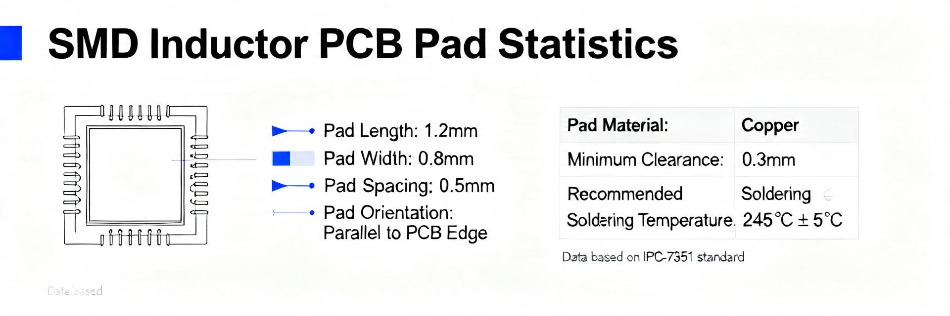
Use relative rules: pad length = terminal exposed length + 10–30% (or +0.25–0.5× terminal width as vendor‑neutral guidance). Aim for pad aspect ratios between 1.2–2.0, fillet target angle >30°, and copper annulus minimums per thermal and mechanical needs. Store these as library presets for quick validation against component metadata.
High-Density Power Converter
Prioritizes thermal dissipation via maximized copper pour and optimized stencil apertures.
Compact Wearable Design
Prioritizes space savings and mechanical fillet strength for drop-test resilience.
Footprint Design Guidelines: Implementation Steps
Capture component dims → choose pad type (NSMD vs SMD) → set solder mask openings → define stencil apertures → run 3D fillet simulation if available → perform DRC/DFM checks. Tag footprint files with metadata (component dims, thermal notes, created_by, version) and adopt semantically versioned filenames to enable controlled library rollouts and traceability.
Step-by-Step Footprint Creation Checklist
- Verify component drawing and terminal geometry.
- Apply empirical pad rule (L+20%).
- Select pad shape (Rounded vs. Chamfered).
- Set solder mask clearance (NSMD preferred for reliability).
- Determine stencil aperture (80-90% paste volume).
- Simulate fillet or perform desktop hand‑solder test.
- Run Final DRC against manufacturing stack-up.
Design Trade-offs: Solderability vs. Electrical/Thermal Needs
Larger pads generally improve solderability but raise thermal mass and potential cold‑joint risk; smaller pads reduce thermal coupling but can compromise fillet. Decide based on product priorities: if mechanical robustness is critical, prioritize pad size and fillet targets; if thermal dissipation or impedance is primary, constrain pad copper and validate via assembly trials.
Assembly & Testing Protocols
Define a minimal validation matrix: sample sizes per lot, at least two reflow profiles (ramp rates and max temp), stencil aperture variants, two paste alloys, and representative PCB finishes. Tests should include IPC‑style fillet inspection, cross‑section analysis, shear/pull testing, thermal cycling and vibration; declare pass/fail thresholds before trials begin.
Summary
- Data-Driven Design: Translate measured reliability data into pad stats and rules to reduce solder‑joint failures.
- Validation: Use empirical benchmarks—fillet coverage, shear strength, and thermal cycling—to qualify footprints.
- Control: Deploy a controlled rollout with library versioning and targeted KPIs to sustain ongoing process health.
FAQ
What are the top pad stats to monitor for SMD inductor footprint validation?
Track solder fillet coverage percentage, solder paste volume per pad from SPI, joint shear strength (N), and yield linked to pad geometry. These metrics correlate strongly with field returns.
How do I choose between NSMD and SMD pads?
Choose NSMD when copper annulus and reliable mechanical fillet are priorities; SMD can be used when pad stability and planarity matter more. Validate choice through a pilot matrix.
What minimal validation matrix should I run before production release?
Run pilot builds across two reflow profiles, two stencil aperture variants, and representative PCB finishes. Perform visual fillet inspection, shear tests, and thermal cycling.


