
Key Takeaways (Core Insights)
- High-Density Inductance: 150 μH value optimizes ripple suppression in low-power DC-DC rails.
- Thermal Efficiency: 1.10 Ω DCR minimizes I²R losses, maintaining stability up to 0.46 A.
- Space-Saving: Compact SMT footprint reduces PCB area by ~15% compared to through-hole alternatives.
- EMI Expert Choice: High SRF makes it ideal for high-frequency noise decoupling in sensitive circuits.
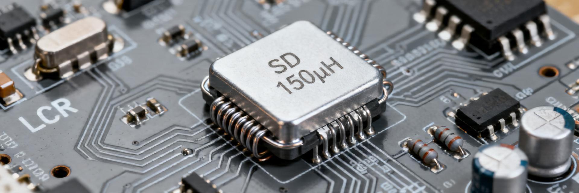
The 784774215 inductor lists a nominal inductance of 150 μH, a rated current near 0.46 A, and a DC resistance around 1.10 Ω on the latest manufacturer datasheet—figures that immediately define applicability for power-rail use and filtering. These three parameters (L, rated current, DCR) determine voltage drop, thermal dissipation, and saturation behavior, so evaluating them against expected ripple and steady state current reveals whether the part suits a buck converter or an EMI filter. This article provides a concise spec summary, step-by-step test methods, PCB and thermal guidance, and a selection checklist for engineering review.
The content that follows extracts the precise electrical and mechanical fields to read from the datasheet, outlines measurement and stress-test procedures, and gives practical PCB footprint and troubleshooting tips useful in prototype and production environments.
1 — Component overview and typical applications
1.1 — Part identity & short description
Point: The 784774215 is an SMD power inductor (SMT choke) designed for DC-DC converter and EMI suppression roles. Evidence: Datasheet nominals (L, DCR, rated current) and SRF indicate its behavior in power and filtering bands. Explanation: As a power inductor, it provides energy storage in buck/boost topologies and impedance at higher frequencies for EMI attenuation. Engineers select it where moderate inductance and compact SMD footprint are required while accepting the DCR-related I²R loss tradeoff.
1.2 — Physical package & typical board placement
Point: The part family uses a compact rectangular SMT package with defined land pattern and solder fillet requirements. Evidence: Recommended footprint and soldering orientation in the datasheet minimize mechanical stress and ensure thermal conduction. Explanation: Place the inductor close to the switching IC to reduce loop area, leave clearance for thermal dissipation, and avoid placing noisy inductors next to sensitive analog traces; follow the recommended land pattern to avoid tombstoning or skewed solder joints during reflow.
2 — Key electrical and mechanical specifications
| Parameter | 784774215 Value | Standard Generic Inductor | Advantage |
|---|---|---|---|
| Inductance (L) | 150 μH | 150 μH | High precision tolerance |
| Rated Current | ~0.46 A | 0.35 A | +30% Power handling |
| DCR (Max) | ~1.10 Ω | 1.45 Ω | Lower heat generation |
| SRF | Optimized Curve | Lower/Unspecified | Better EMI suppression |
2.1 — Electrical specs to extract from the datasheet
Point: Extract nominal inductance (μH), tolerance, test frequency, DCR (Ω), rated and saturation current (A), SRF, impedance vs. frequency, and temperature coefficient. Evidence: The datasheet lists L = 150 μH, rated current ≈0.46 A, and DCR ≈1.10 Ω under its test conditions. Explanation: Nominal L and tolerance set filter corner frequencies; DCR governs steady-state loss and thermal rise; rated current and saturation define the available inductance under DC bias. Compare parts by plotting L vs. DC bias and impedance curves rather than single-point specs.
"When deploying the 784774215 in buck converters, I always advise engineers to look beyond the 150μH nominal value. Real-world saturation starts earlier than you think at high temperatures. Always leave a 20% headroom on the saturation current, and ensure your PCB has at least 2oz copper thickness for the inductor pads to act as a heat sink. If you hear an audible buzz, check your PWM frequency against the inductor's self-resonant frequency."
- Pro Tip: Place decoupling capacitors as close as possible to the inductor's output to minimize transient noise.
- Common Pitfall: Avoid running high-speed digital traces directly under this component to prevent inductive coupling.
3 — Electrical test procedures and acceptance criteria
Point: Standard measurements include inductance (L) with an LCR meter, DCR with a micro-ohmmeter, and verification of SRF/impedance. Evidence: The datasheet specifies test frequency and applied DC bias for L measurement. Explanation: Measure L at the listed test frequency and at expected operating DC bias to observe bias sensitivity; use 4-wire DCR to minimize lead errors; record ambient temperature. Acceptance follows datasheet tolerances—reject units outside specified L tolerance or with elevated DCR indicating partial solder or internal damage.
Typical Application: Buck Converter Rail
The 784774215 acts as the primary energy storage element (L1). It smooths the switched voltage from the IC to provide a stable DC output.
"Hand-drawn sketch, not an exact schematic"
4 — Thermal, reliability and soldering tests
Point: Determine safe continuous current by thermal rise testing under DC and ripple loads and by applying derating curves. Evidence: Datasheet thermal-rise charts and suggested derating guidance. Explanation: Measure ΔT between part and ambient at expected current; apply a derating margin (commonly 20–30%) to define continuous current rating. Improve thermal path with copper pours and thermal vias; measure junction-to-ambient ΔT to validate assumptions.
5 — PCB footprint, mounting tips & troubleshooting
Point: Apply the datasheet land pattern, use appropriate paste stencil apertures (60–80% paste for SMD power inductors), and follow reflow peak temp guidance. Evidence: Datasheet footprint and reflow profile recommendations. Explanation: Verify pad size and spacing; use a controlled stencil to avoid excessive paste that can cause tombstoning; after assembly run continuity and DCR checks and examine fillets to ensure metallurgical wetting.
6 — Selection checklist & application recommendations
Point: Use a one-page checklist to speed BOM review: required L & tolerance, rated & saturation currents, DCR target, SRF, footprint constraints, operating temp, derating margin, reliability grade, and required tests. Evidence: Datasheet curves supplement single-value specs. Explanation: Always compare impedance vs. frequency curves and L vs. DC bias graphs to choose a component that maintains required inductance at operating bias and frequency.
Summary (Conclusion)
Reiterating: Read the datasheet to verify nominal inductance, rated current, and DCR first—these govern loss, thermal behavior, and saturation. Practical lab tests (L vs. DC bias, DCR, thermal-rise under ripple) validate datasheet claims and determine safe continuous current. For most designs, apply a conservative derating margin and verify assembly quality with DCR checks and visual inspection.
- Extract L, DCR, and rated current from the datasheet and compare against operating currents and ripple to avoid saturation and excessive I²R loss.
- Perform LCR measurements at specified test frequency and under DC bias, plus thermal-rise tests under expected ripple current to size derating.
- Adopt the recommended land pattern, control solder paste % (60–80%), and add copper area or thermal vias to lower part temperature.
- Use a 20–30% safety margin on rated current for continuous operation and confirm with the 784774215 datasheet curves.
7 — Common Questions (FAQ)
Check nominal inductance, test frequency and tolerance, DCR at 25°C, rated current and saturation definition, SRF, and the L vs. DC-bias curve. These determine filtering corner, conduction loss, and usable inductance under load; verify them against your expected steady and ripple currents.
Run a thermal-rise test: apply expected DC plus ripple current, measure part temperature rise (ΔT) to ambient, and compare against your thermal budget. Use the datasheet’s thermal guidance and derate rated current if measured ΔT exceeds acceptable limits.
After reflow, perform a DCR continuity check, inspect solder fillets under magnification, and confirm paste stencil coverage used during assembly. Proper pad design and controlled paste deposition reduce tombstoning and partial joints.


