
A technical guide for designers balancing inductance, thermal limits, and efficiency in low-power DC-DC converters.
The 784774139 power inductor lists a nominal inductance of 39 µH ±15%, a rated current near 0.94 A, an operating temperature range of −40 to 125 °C, and a typical low milliohm DC resistance (DCR) on its datasheet and lab measurements. These specs matter because the modest inductance and sub‑1 A rating force designers to balance I²R winding losses, frequency‑dependent core losses at switching speed, and saturation margin when used in low‑power DC‑DC converters.
This article walks engineers through actionable spec checks, loss calculations, thermal testing, PCB layout guidance, and selection criteria so a design team can validate the 784774139 inductor for production use. Emphasis is on measurement methods (Kelvin DCR, impedance sweeps), loss decomposition (I²R vs core), thermal modeling (θJA), and practical derating rules.
(1) Product background & key specs — 784774139 at a glance
Electrical specifications — what to list and why
Report these electrical specs and verify them by test: nominal inductance (39 µH ±15%), DCR typical and max (mΩ), rated current and saturation current (Isat at specified ΔL), self‑resonant frequency (SRF), impedance vs frequency curve, and frequency/temperature behavior. DCR governs I²R loss; SRF limits usable switching harmonics; Isat defines margin against inductance collapse under DC bias.
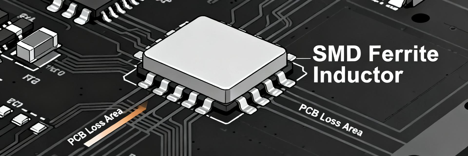
Mechanical & environmental specs — layout constraints
Capture package size, recommended land pattern, SMD mounting style, core material (ferrite), maximum operating temperature, and soldering profile limits. These mechanical specs influence thermal dissipation (board copper area, fillets) and reliability under vibration/thermal cycling.
(2) Electrical performance & loss mechanisms (detailed analysis)
DC/winding losses (I^2R) — measurement & calculation
Calculate DC winding loss as P_DCR = I_rms^2 × DCR where I_rms includes DC and ripple components. Measure DCR with a 4‑wire Kelvin method at 20 °C and record sample spread; correct DCR for operating temperature using the copper temperature coefficient (~0.4%/°C) to predict in‑situ I²R loss. Practical tip: measure multiple units and set acceptance limits based on mean±3σ.
AC/core losses & frequency dependence
Core losses stem from hysteresis and eddy currents and scale with flux swing ΔB and frequency. At switching frequencies, core loss can rival or exceed I²R loss when ripple current or switching frequency is high. Measure impedance vs frequency with an LCR/impedance analyzer and perform calorimetric or instrumented converter tests to capture total loss under realistic PWM waveforms.
(3) Thermal behavior, derating & saturation
Thermal modeling
Set up thermal tests with controlled ambient, proper board mounting, and thermal imaging to measure temperature rise versus power. Derive θJA by applying known loss and measuring ΔT between part and ambient. Combine calculated losses (I²R + core) with θJA to estimate steady‑state temperature and add safety margin (typically 10–20 °C).
Current derating & saturation
Differentiate rated current (thermal limit) from saturation current (magnetic limit). Generate a derating curve by ramping DC current while monitoring inductance drop: plot L vs DC bias and note Isat where L falls by a specified percentage (e.g., 30%). For continuous operation, apply conservative derating (e.g., ≤70% of rated current).
(4) PCB layout, EMI considerations & test protocols
Keep traces to switching nodes short, maximize thermal copper under SMD pads, and ensure solder fillets for heat transfer. Place the inductor to minimize loop area of switching node to reduce EMI; locate sensitive analog circuits away from the switching node. If EMI persists, consider common‑mode filtering or careful ground stitching.
Bench test protocol: how to measure in situ
Measure L with an LCR meter at relevant frequency and under DC bias; perform impedance sweeps to find SRF. For converter loss testing, use a current probe and sense resistor to capture ripple and I_rms, and measure temperature rise with a thermal camera or calorimeter.
(5) Application notes, selection checklist & alternatives
Example: For a step‑down converter at fs = 500 kHz with Vout and duty D, estimate ripple ΔI = Vout*(1−D)/(L*fs) using L=39 µH. Compute I_rms from DC and ripple, then estimate P_DCR. Verify SRF above switching harmonics and ensure Isat margin for peak currents.
Conclusion & Recommended Actions
In summary, the 784774139 power inductor (39 µH ±15%, ~0.94 A rated, ferrite SMD) shows that the dominant losses are I²R winding losses and frequency‑dependent core losses. Recommended actions: measure DCR at operating temperature, perform impedance and L vs DC bias sweeps, derive θJA from thermal testing, and build derating curves.
Key Summary
- Calculate I²R loss from measured DCR and include ripple current in I_rms to size thermal margins.
- Core losses rise with frequency; use impedance sweeps and calorimetric tests to separate core vs winding losses.
- Derive θJA from on‑board thermal tests; apply conservative derating (e.g., ≤70% rated current) in high ambient conditions.
Frequently Asked Questions
What are the key specs to verify for 784774139 before selection?
Verify nominal inductance and tolerance, DCR at 20 °C, rated and saturation currents, SRF, and thermal/soldering limits.
How should I measure losses and separate I^2R from core losses?
Measure DCR at 20 °C and correct for temperature for I²R. Subtract this from total measured loss (via calorimeter) to estimate core loss.
What thermal derating rules apply?
Derive θJA on the target PCB and target ≤70% of rated current in elevated ambient conditions to ensure reliability.


