
Actionable guidance for power conversion, EMI suppression, and PCB integration.
The 784774122 datasheet lists nominal inductance at 22 µH, rated current near 1.28 A, and a DC resistance around 0.18 Ω—figures that position the part for low-to-moderate current power conversion and EMI suppression. This article converts those headline numbers into actionable guidance: how to read the electrical data, validate performance on the bench, and integrate the component into PCB designs while avoiding common pitfalls.
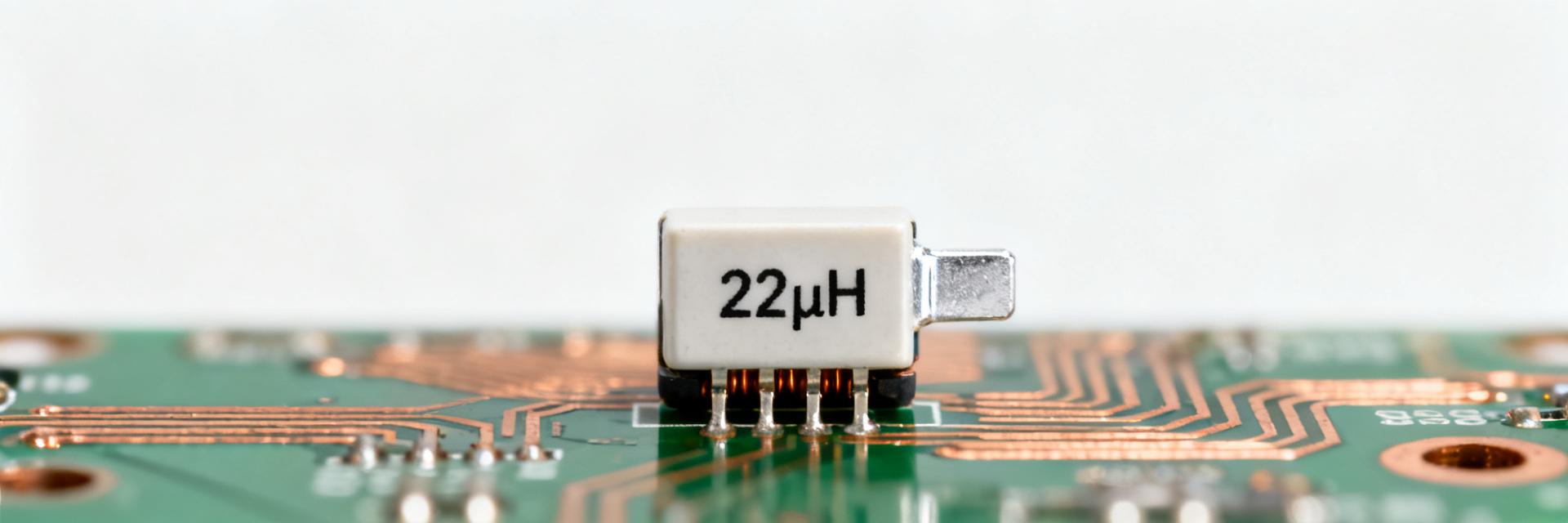
01 Quick overview: What the 784774122 datasheet reveals (background)
Key electrical specs at a glance
The datasheet provides the core electrical specs designers need: nominal inductance 22 µH ± tolerance, rated DC current ~1.28 A, DCR ≈ 0.18 Ω, and a reported self-resonant frequency (SRF). Understanding these electrical specs clarifies suitability for buck outputs, input filters, or EMI chokes; refer to the datasheet table and figure numbers for exact curves and impedance points.
Mechanical and thermal notes
The part is an SMD power inductor with a defined recommended land pattern and height/footprint dimensions; the datasheet includes mechanical drawings and pad recommendations—refer to the mechanical drawing and land pattern figures. Maximum operating temperature and soldering profile are specified; follow the recommended reflow profile and pad size to avoid thermal/mechanical stress during assembly.
02 Deep electrical specs analysis (data analysis)
Frequency response and impedance behavior
Reading inductance vs. frequency and impedance curves reveals SRF and usable inductive bandwidth. In inductor analysis, designers pick the frequency range where X_L >> ESR and below SRF. Typical switching frequencies (100 kHz–2 MHz) span regions where inductive reactance varies strongly; use the plotted L(f) curve in the datasheet figures to extract usable bandwidth.
| Frequency | Approx. L (µH) | Comment |
|---|---|---|
| 100 kHz | 22.0 | Nominal inductance for DC-DC output |
| 500 kHz | 20.5 | Small reduction from DC bias effects |
| 1 MHz | 17.0 | Approaching reduced reactance |
| 5 MHz | 5.0 | Near SRF region—avoid for inductive use |
Current handling, saturation and thermal derating
Datasheet L vs. I curves show how inductance collapses with DC bias; rated current differs from saturation current and thermal limits. Use conservative derating (50–80% of rated current) depending on cooling and ambient temperature. Losses are I^2·R: for example, 1.0 A DC gives loss ≈1.0^2·0.18 = 0.18 W—estimate temperature rise using board thermal impedance or a thermal camera during validation.
Measured performance vs datasheet: Practical bench tests
Recommended test methods and setups
Use an LCR meter or impedance analyzer for frequency sweeps, with open/short calibration and a low-inductance fixture. For DC-bias inductance, use a current source while measuring L at the intended switching frequency. Measure DCR with a Kelvin ohmmeter. Thermal rise tests use steady current with infrared imaging or thermocouples after burn-in to capture realistic operating temperature.
Interpreting deviations and acceptable tolerances
Common deviations arise from fixture parasitics, soldering, and temperature. Accept L within ±10–20% depending on the indicated tolerance; DCR should be within specified tolerance bands. If measurements deviate: re-check fixture calibration, measure on-board vs component-alone, and verify solder fillet quality and PCB pad dimensions per the datasheet land pattern.
Application guidance and PCB integration
Typical use cases and selection criteria
With 22 µH and ~1.28 A rating, the component suits buck converter outputs for low-current rails, input EMI suppression, and general-purpose filtering. Selection rules: prioritize lower DCR when loss budget is tight, higher inductance for lower ripple at a given switching frequency, and ensure SRF sits above the highest harmonic of interest for stable inductor behavior.
Layout, thermal management and EMI best practices
Place the inductor close to the switching node or input source depending on its role, keep traces short, and avoid routing sensitive return currents beneath the choke. Use copper pours and thermal vias to spread heat; stitch ground around switching loops to reduce EMI. Validate thermal performance with populated prototypes and adjust copper area or add vias under pads if hot spots appear.
Quick selection checklist
- Required inductance at operating frequency
- Allowable DCR and loss budget
- Saturation/peak current margin
- SRF above switching harmonics
- Mechanical fit and reflow compatibility
- Locate datapoints in L vs I / L vs f figures
Common failure modes
- Audible/conducted noise (Saturation)
- Overheating (Excess I^2·R loss)
- Mechanical cracking (Poor reflow)
- Diagnose with scope & thermal imaging
- Mitigate with higher Isat or cooling
- Correct footprint & soldering
Summary
- The 784774122 datasheet provides key electrical specs—22 µH, ~1.28 A, ~0.18 Ω—that indicate suitability for low-to-moderate power and EMI roles; interpret frequency and L-vs-I curves to confirm fit.
- Bench validation requires calibrated LCR/impedance sweeps, Kelvin DCR checks, and thermal imaging; accept reasonable tolerance deviations and re-test with corrected fixturing as needed.
- For PCB integration, minimize loop area, use copper for thermal spreading, respect the recommended land pattern, and derate current based on thermal environment and SRF considerations.
SEO & editorial guidelines
Target concise, data-driven content for US design engineers. Use the official datasheet figures and tables for numeric references (cite the datasheet PDF and figure/table numbers in internal review). Include one annotated L vs frequency table, one thermal/loss example, and keep phrasing technical and precise.Frequently Asked Questions
How accurate are the inductance values in the 784774122 datasheet under DC bias?
Nominal inductance values are measured without DC bias; the datasheet includes L vs I curves showing typical reduction under DC current. Expect notable L reduction as DC approaches saturation; design with margin (50–80% of rated current) and validate with an L vs I sweep on an impedance analyzer to confirm usable inductance at operating bias.
What test procedure verifies DCR and thermal performance for the 784774122 datasheet values?
Measure DCR using a four-wire Kelvin method at controlled ambient temperature, then run a steady-state current equal to expected operating current while monitoring temperature with a thermocouple or IR camera. Compare measured DCR and temperature rise to datasheet curves and adjust copper area or derating if thermal rise exceeds acceptable limits.
How should engineers interpret SRF and impedance data from the 784774122 datasheet for switching converters?
Use impedance curves to identify SRF and ensure the switching fundamental and major harmonics are below SRF for inductive behavior. If harmonics approach SRF, expect reduced reactance and possible resonance; either choose a part with higher SRF or redesign the filter topology to maintain stable converter loops and EMI performance.


