
In validation labs for power-supply components, inductance drift under DC bias and thermal stress is the single biggest source of margin loss. This technical brief provides an engineering-grade analysis of the 784774115 15µH inductor.
This article focuses on the 784774115 and the 15µH inductor form factor, summarizing critical specs and the test protocols engineers need to validate performance and reliability for production. Content is written for US power-design engineers who require actionable test procedures, clear pass/fail criteria, and practical PCB and procurement checklists. The guidance emphasizes repeatable measurements, statistical sampling, and how to interpret degradation metrics for volume release.
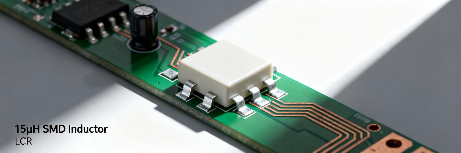
1 — Background & Part Overview
1.1 Key datasheet specs at a glance
Point: The datasheet headline fields define suitability for a power design. Evidence: Extract nominal inductance (15µH), tolerance, rated current (I_RMS), saturation current (I_sat / I_Loss%), DCR, SRF, operating temperature range, package/footprint, mounting style, and qualification level. Explanation: Present these as a short table and note all test conditions (ambient temperature, humidity) used by the vendor so lab measurements are comparable.
| Parameter | Typical Entry / Note |
|---|---|
| Nominal inductance | 15 µH |
| Tolerance | Specify per datasheet (e.g., ±20%) |
| Rated current (I_RMS) | Vendor value — verify by DC bias test |
| DCR | Check at 20°C; impacts efficiency & thermal rise |
| SRF | Self‑resonant frequency — defines HF limits |
1.2 Typical applications & where this 15µH inductor fits
Point: A 15µH SMD inductor typically targets DC‑DC converters, power filtering and EMI suppression in mid‑power rails. Evidence: It suits buck/boost converters handling low- to mid‑ampere ranges and filters in power‑supply input stages. Explanation: Use 15µH when switching frequency, required ripple current, and needed impedance at switching harmonics favor higher inductance versus smaller values; choose lower inductance when size or saturation margin is limiting.
2 — Deep Specifications: Electrical & Mechanical Details
2.1 Electrical behaviour: inductance vs frequency, DC bias & SRF
Characterize inductance across frequency and under DC bias to understand in‑circuit behavior. Evidence includes producing L(f) curves and L vs DC current tables; measure SRF and DCR with an impedance analyzer or LCR meter under specified temperature. These inductor specs determine efficiency and thermal rise — DCR drives I²R loss, DC bias reduces effective inductance, and SRF sets the upper usable frequency.
2.2 Mechanical, thermal & environmental limits
Mechanical and thermal constraints drive mounting and handling rules. Evidence is based on reference package dimensions, recommended PCB footprint, reflow profile, maximum operating and storage temperatures, and vibration/shock limits from the datasheet. Proper footprint, generous copper for heat spreading, and controlled soldering profile reduce solder‑joint fatigue and thermal delamination risks in production boards.
3 — Test Methodology: How to Verify Specs in the Lab
3.1 Bench tests to validate electrical specs
Define repeatable bench procedures for core electrical measurements. Use an impedance analyzer or precision LCR meter for L(f) sweep, apply incremental DC bias (e.g., 0→I_RMS in steps) allowing stabilization time at each step, measure DCR with a four‑wire ohmmeter, and find SRF via network analysis. Log raw data, note fixture parasitics, test multiple samples per lot, and record pass/fail against datasheet limits and design margins.
| Measurement | Condition | Pass / Fail |
|---|---|---|
| Inductance @ 100 kHz | 0 A DC bias, 20°C | Within tolerance |
| Inductance @ I_RMS | Stabilized after 60 s at rated current | > specified I_Loss% |
| DCR | 4‑wire, 20°C | ≤ datasheet + tolerance |
3.2 Environmental & mechanical testing protocols
Use standardized stress tests to reveal degradation modes. Evidence includes running thermal cycling, HTOL, damp‑heat, solderability, shock and vibration per industry standards and record inductance shift, DCR change, and visual defects. Define pass/fail thresholds (e.g., ≤5% inductance shift, ≤10% DCR increase) and log failed samples for root‑cause analysis.
4 — Reliability, Failure Modes & Data Interpretation
4.1 Common failure modes and root-cause indicators
Know the typical failure modes to interpret test data. Magnetic core saturation shows as large L drop under DC bias; insulation breakdown or shorts appear as DCR decrease or catastrophic open; solder fatigue shows intermittent connectivity and visual joint cracks. Combine electrical signatures with cross‑section or X‑ray to confirm mechanical or material root causes and guide corrective actions.
4.2 Accelerated testing, statistical lifetime estimates & derating rules
Translate accelerated stresses into field lifetime estimates. Evidence comes from applying Arrhenius for thermal degradation and thermal cycling models for mechanical fatigue; test sample sizes that support 90% confidence intervals and report MTBF or usable lifetime windows. Recommend conservative derating — limit continuous current to a fraction of rated current and maintain temperature margin to reduce in‑field failures.
5 — Practical Selection, PCB Integration & Qualification Checklist
5.1 Layout, thermal management and derating tips
Layout determines thermal and mechanical robustness. Use recommended pad geometry, multiple thermal vias under and adjacent to the part, pour copper to spread heat, and avoid placing the inductor next to hot components. For continuous operation, derate current by a practical margin (e.g., 20–30%) depending on allowed temperature rise and measured thermal impedance.
5.2 Procurement, incoming inspection & qualification checklist
A strict incoming and qualification flow prevents lot surprises. Verify datasheet fields on first article parts, run sample tests (inductance, DCR, visual, solderability), implement lot acceptance sampling, and require traceability documentation. Produce a short tech pack for suppliers specifying required tests, acceptance criteria, and reporting frequency to keep manufacturing quality consistent.
Summary
- The 784774115 15µH inductor requires explicit verification of inductance vs DC bias and SRF to ensure design margins; measure with calibrated LCR/impedance equipment under documented conditions.
- Thermal and mechanical constraints (DCR, reflow profile, PCB copper) drive in‑field reliability; apply conservative current derating and heat‑spreading layout rules to limit thermal rise.
- Qualification must combine electrical bench tests and accelerated environmental stresses with a statistical sampling plan and clear pass/fail thresholds to support volume release.
Frequently Asked Questions
How should an engineer test the 784774115 inductance vs DC bias?
Measure inductance using an impedance analyzer while applying incremental DC current steps up to and beyond rated current, allowing stabilization (30–60 seconds) at each step. Record L and temperature; normalize results to the datasheet conditions to identify percent loss at operating current and to determine usable current derating.
What are acceptable limits for DCR change after environmental stress for the 15µH inductor?
Acceptable DCR increase is typically small; a practical pass criterion is ≤10% increase after thermal cycling or humidity exposure. Larger increases indicate corrosion, solder joint issues, or internal damage and require destructive analysis to confirm root cause and corrective action.
How many samples are recommended for lot qualification of the 784774115?
A common approach is AQL‑based sampling for incoming lots combined with a 30‑sample accelerated test cohort for reliability estimates. For lifetime claims, use larger groups sized to provide ≥90% confidence in accelerated models; document sample selection and statistical methods in the qualification report.


