
Key Point: The device is specified with 15 µH nominal inductance, a rated current of 1.2 A, DCR ≈ 235 mΩ, and an operating range near −40 °C to +125 °C, making it a common choice for power-filter and low-power buck converter circuits.
Evidence: These metrics derive from the manufacturer datasheet and typical test conditions.
Explanation: For compact designs the combination of moderate inductance and modest current rating frames performance trade-offs between ripple suppression, loss, and saturation headroom.
The introduction frames why this family is relevant for small power designs. Test-frequency and DCR numbers indicate likely efficiency and thermal rise at converter operating points. Writers should treat these baseline numbers as starting points for layout, derating, and validation planning when targeting sub-2 A rail applications.
1 — Quick technical overview (background)
Typical electrical identity & role
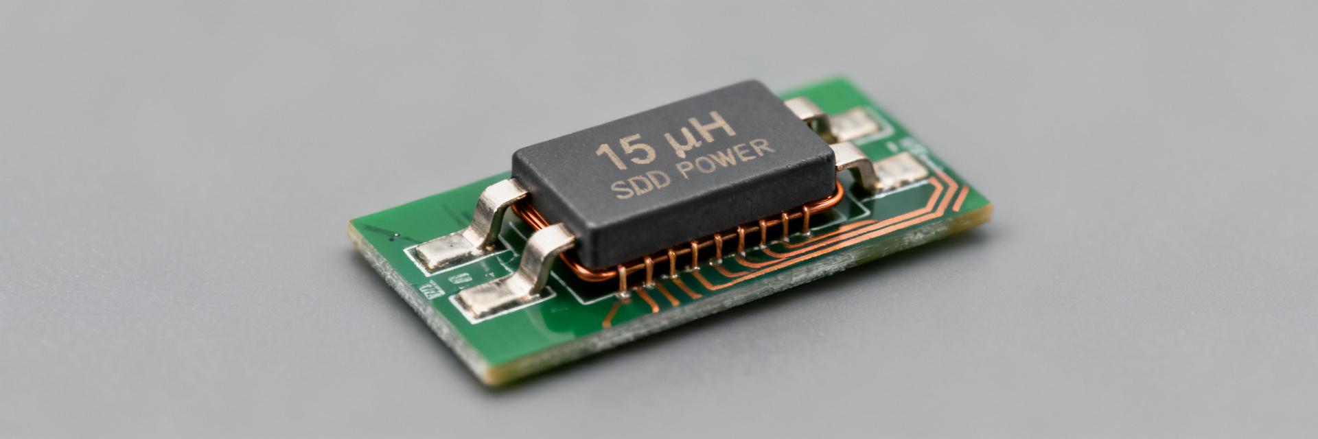
Point: An SMD power inductor stores energy and shapes current ripple on switching rails.
Evidence: A 15 µH, 1.2 A device typically sits in low-power buck converters or post-regulator LC filters.
Explanation: Nominal inductance controls ripple amplitude, the current rating sets continuous headroom, and DCR governs I²R loss; mapping those specs to converter equations yields expected ripple and loss figures for selection.
Package, footprint and mechanical notes
Point: The part uses a compact SMD construction such as a drum-core/wirewound style with a small footprint class.
Evidence: Typical footprint considerations include pad spacing, height, and mass that appear in the datasheet land-pattern recommendations.
Explanation: For dense PCBs designers must account for component height, solder fillet reliability, and pad size; tight clearances may limit current-carrying copper and thermal dissipation in space-constrained layouts.
2 — Datasheet deep-dive: electrical and thermal specs (data analysis)
Core electrical specs to extract and compare
Point: Key datasheet numbers to capture are nominal inductance, tolerance, test frequency, rated current, saturation current, DCR, and SRF. Evidence: For a 15 µH device the rated current of 1.2 A and DCR ≈ 235 mΩ dominate thermal and efficiency calculations. Explanation: Use I²R for steady-state copper loss, check Isat to avoid inductance collapse under peak currents, and confirm SRF to ensure the inductor behaves inductively across the converter’s switching band.
Thermal, environmental & reliability specs
Point: Operating and storage temperature ranges, maximum part temperature during reflow, and recommended derating determine reliability. Evidence: The datasheet specifies reflow profiles and a −40 °C to +125 °C operating window; designers must apply derating in constrained thermal cases. Explanation: A practical rule is to derate continuous current to 70–80% of rated when ambient or adjacent heating is present to limit temperature rise and preserve inductance and core life.
3 — Performance characteristics and real-world behavior (data analysis)
Frequency response, impedance, and saturation behavior
Point: L(f) and impedance curves reveal where inductance falls near saturation and SRF, affecting EMI and filter effectiveness. Evidence: Measured curves under DC bias show the inductance reduction as DC current increases and the SRF where capacitive behavior begins. Explanation: Report L at relevant DC bias and switching frequency, note impedance magnitude, and state where the device ceases to provide expected attenuation to guide filter placement.
Loss mechanisms and efficiency impact
Point: Losses stem from DCR (I²R) and frequency-dependent core loss; both affect converter efficiency. Evidence: The dominant steady loss approximates P_loss ≈ I_rms² × DCR; core loss grows with frequency and flux swing. Explanation: Include example calculations for converter points (e.g., 0.5 A DC with 1 A ripple) to quantify losses and compare alternative inductors for minimal efficiency impact.
5 — Testing, troubleshooting & procurement tips (action)
Bench tests and validation protocol
Point: Validate the inductor with targeted bench tests: inductance under DC bias, DCR, saturation curve, thermal-rise at rated current, and impedance sweep for EMI. Evidence: Compare measured L and DCR against datasheet limits and record thermal rise with representative PCB mounting. Explanation: Define pass/fail thresholds per datasheet tolerances and include margin checks; failing L under bias or excessive temperature rise indicates the need for higher Isat or lower DCR options.
Sourcing, part cross-reference and ordering considerations
Point: Verify part identity by matching inductance, current rating, DCR, package, and reflow spec before ordering. Evidence: Part numbers and datasheet pages provide the definitive specs and land-patterns; lifecycle and lead-time risks can affect availability. Explanation: When procuring, confirm the latest datasheet and qualification status, plan minimum order quantities and lead times, and maintain cross-reference notes for future substitutions.
Summary
Point: The 15 µH device balances compact size with moderate current capability and measurable DCR losses. Evidence: With ~1.2 A rated current and ≈235 mΩ DCR, the trade-offs favor low-power buck filters rather than high-current regulators. Explanation: Designers should prioritize current derating, DCR-driven loss evaluation, and careful layout to secure reliable in-field performance.
Key Summary
- The 784773115 part delivers 15 µH nominal inductance with ~1.2 A rated current; designers should derate continuous current to around 70–80% in constrained thermal environments to protect performance and lifetime.
- DCR (~235 mΩ) drives steady losses; estimate copper loss with P_loss ≈ I_rms² × DCR and compare against converter efficiency targets when selecting the inductor for a buck regulator.
- Verify SRF and Isat from the manufacturer datasheet, measure L under DC bias during bench validation, and follow recommended land-pattern and reflow guidelines to minimize EMI and thermal issues.
6 — Common questions and answers (FAQ)
What tests validate the 784773115 performance in a buck converter?
Perform L measurement under representative DC bias, DCR verification, saturation check by plotting L versus ID, thermal-rise test at expected operating current on the target PCB, and an impedance sweep across switching frequencies to validate EMI behavior; compare all results to datasheet tolerances for pass/fail decisions.
How much should continuous current be derated for reliable operation?
Derate continuous current to roughly 70–80% of the rated value in high ambient or thermally constrained designs to limit temperature rise and avoid long-term degradation; use thermal-rise tests on the actual PCB to refine the derating percentage for the specific implementation.
What are the most common causes of unexpected loss with SMD power inductors?
Unexpected loss most often arises from underestimated DCR-related I²R dissipation, core loss at higher switching frequencies, poor PCB thermal conduction, and partial saturation from transient peaks; quantify each by measurement and eliminate layout or margin shortfalls to improve efficiency.


